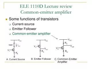
Common Emitter Amplifier
Common Emitter Amplifier. Design Rules. V RE should be > 100 mV. Design Procedure. Decide on an IC that yield to proper gm and r π . Choose a proper I C R E , e.g. 200 mV. Determine Vx given IC and I C R E . Choose R1 and R2 to provide necessary value of VX and establish I1>>IB.

Common Emitter Amplifier
E N D
Presentation Transcript
Design Rules VRE should be > 100 mV.
Design Procedure • Decide on an IC that yield to proper gm and rπ. • Choose a proper ICRE, e.g. 200 mV. • Determine Vx given IC and ICRE. • Choose R1 and R2 to provide necessary value of VX and establish I1>>IB. • Select an RC to place the transistor at the edge of saturation.
Example 1 • Specification • gm=19.2 mS→IC=0.5 mA • Assume that VRE=200 mV. • RE=0.2 V/IC=400 Ohms • Calculate VBE • VBE=VTln(IC/IS), IS=6.734x10⁻¹⁵ A→VBE=0.65 V • Calculate VX=VBE+VRE=0.65+0.2V=0.85 V
Example 1(Cont.) • IC=0.5 mA, β=150→ IB=3.33 uA • I1>>IB. Let’s say that I1=40IB. →I1=133.3 uA • Assume that VCC=12 V. →R1+R2=VCC/I1→R1+R2=90 KOhms • Vx=VBE+RE*IC=R2*VCC/(R1+R2)→R2=6.38 KOhm • R1=(R1+R2)-R2=90 Kohms-6.38 Kohms=83.619 Kohms • Place Q1 at the edge of Saturation: VCC-RC*IC=VX→RC=22.30 KOhms
Sensitivity to Component Variation 1% error in R3 leads to 3 % error in IC. 5% error in R3 leads to 12.5 % error in IC.
Increase VRE to 400 mV 1% error in R3 leads to 2.3 % error in IC. 5% error in R3 leads to 9.9 % error in IC.
Trade-Off • As VRE increases, the circuit becomes slightly less sensitive to Resistor variation • But VCE also drops, increasing the likely hood that the circuit can be driven into saturation.
Input and Output Vout, m=46 mV Vin, m=1 mV
Replace the transistor by its small signal equivalent circuit (EQ 5.157) Comparision:ADS Simulation: 46 EQ 5.157: 49.33
Idea: Apply degeneration to the biasing, but not to the signal! Zc at 1 KHz: 159.2 mOhms
Input Impedance • Derivation of Input Impedance of Degenerated CE Stage • Input Resistance with no emitter resistance • Input Impedance with Base Resistance • Input Impedance with Bias Resistors included
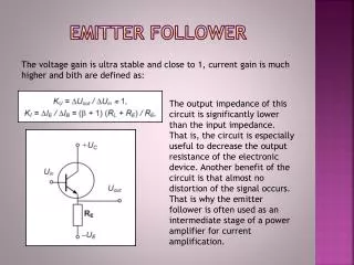
Input Impedance of the Degenerated CE Stage Interpretation: Any impedance tied between the emitter and ground is multiplied by (Beta+1) when seen from the base.
Input Resistance without Emitter Degeneration Resistor Rin=rπ
Output Impedance • Derivation of Output Impedance with Emitter Degeneration Resistance • Output Impedance without Emitter Degeneration Resistance
Without Emitter Degeneration Rout=ro
Gain Modification • Gain of a Degenerated Common-Emitter Amplifier • Without Emitter Degeneration • Gain with a base resistance • Gain with biasing resistors
Voltage Gain Analytical: 13.80 ADS Simulation: 13.4