Basic Electronics
CHAPTER. Basic Electronics. 6. Instructor Name: (Your Name ). Learning Objectives. List the various types of resistors Determine whether a diode is forward biased or reverse biased in a circuit Test a diode with a DMM Explain the function of a zener diode

Basic Electronics
E N D
Presentation Transcript
CHAPTER Basic Electronics 6 Instructor Name:(Your Name)
Learning Objectives • List the various types of resistors • Determine whether a diode is forward biased or reverse biased in a circuit • Test a diode with a DMM • Explain the function of a zener diode • Describe the operation of a bipolar transistor • Explain the difference between a transistor being used as an amplifier and a transistor being used as a relay or a switch
Learning Objectives (continued) • Describe the operation of a field effect transistor (FET) • Discuss the concept of a high side driver and a low side driver
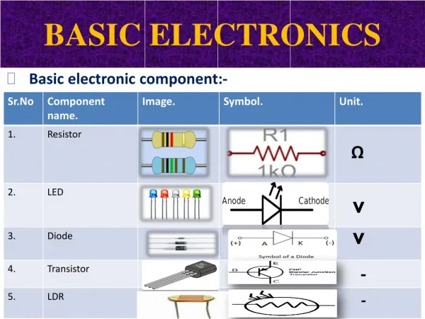
Resistors • Limit the current flow through a circuit • Divide voltage • Give off heat • Two main types of resistors; fixed and variable
Fixed Resistors and Color Code Figure 6-1 Fixed-value resistors: physical size of resistor increases as wattage rating of resistor increases. Figure 6-2 Resistor color code.
Stepped Value Variable Resistor Figure 6-3 Stepped-value resistor network.
Infinitely Variable Resistor Figure 6-4 Infinitely variable resistor.
Potentiometer Figure 6-7 Potentiometer.
Semiconductors • A material that is neither a good nor a poor conductor • Silicon is the most common used in electronics • Semiconductors usually have a negative temperature coefficient (NTC) • Pure silicon has four valence electrons • Impurities added to silicone is a process called doping • Doping with a material that has excessive electrons creates an N-type junction • Doping with a material that has excessive holes creates a P-type junction
N-Type Semiconductor Doped With Arsenic Figure 6-9 N-Type semiconductor doped with arsenic (As).
P-Type Semiconductor Doped With Boron Figure 6-10 P-Type semiconductor doped with boron (B).
Diodes • Two terminal semiconductor that acts as a one way check valve to current flow • The schematic symbol of a diode shows the direction of current flow through the device • If a diode is inserted in a circuit so that it allows current flow it is forward biased • If a diode is inserted in a circuit so that is does not allow current flow it is reversed biased • The positive terminal of a diode is the anode • The negative terminal of a diode the cathode
Diode and Schematic Symbol Figure 6-15 Stripe indicates cathode end of diode. Figure 6-12 Diode voltage.
Diodes (continued) • Diodes will not permit current flow in the forward bias direction until 0.7V is dropped across the diode • A diode will always drop approximately 0.7V regardless of the current or voltage in the circuit • Diodes have a rated limit to reverse bias voltage called the inverse voltage rating • If the inverse voltage rating is exceeded the diode will be destroyed
Diode Testing With a DMM Figure 6-19 Diode testing using DMM.
Light-Emitting Diodes Figure 6-21 Schematic symbol for LED.
Zener Diode • In the forward biased direction zener diodes act like a regular diode and allow current flow • A zener diode has a rating referred to the zener voltage • Once the zener voltage is reached in the reverse bias direction the zener will switch on and conduct current in the reversed bias direction
Bipolar Transistors • Bipolar transistors are made up of P-type and N-type junctions • There are two major types of bipolar transistors PNP and NPN • A PNP type is like a sandwich of N-type material between two slices of P-type material • An NPN type is like a sandwich of P-type material between two slices of N-type material
NPN Bipolar Transistor Figure 6-26 NPN bipolar transistor.
Bipolar Transistors (continued) • The P-type layer of an NPN transistor is the base • One of the N-type layers is called the emitter • The other N-type layer is called the collector • The emitter, collector, and base are labeled E, C, and B • Transistors amplify low level signals to a higher level signal • Transistors act as switches similar to a relay
Bipolar Transistors (continued) • The collector of a bipolar transistor is connected to the positive terminal of the supply voltage • The base of a bipolar transistor is connected to the small signal that will be amplified • The emitter of a bipolar transistor is connected to the load device and the load is connected to the negative terminal of the supply voltage
Transistor Amplifying the Base Current Figure 6-28 Transistor amplifying the base current.
NPN Transistor Used As a Switch Figure 6-29 NPN transistor used as a switch.
Transistors Connected as a Darlington Pair Figure 6-30 Darlington pair permits a very small current to control a very large current.
Field Effect Transistors (FET) • FET’s are controlled by voltage not current • The drain of an FET corresponds to the collector of a bipolar transistor • The gate of an FET corresponds to the base of a bipolar transistor • The source of an FET corresponds to the emitter of a bipolar transistor • The voltage difference between the gate and the source voltage controls the resistance between the drain and the source
N-Channel JFET Schematic Symbol Figure 6-31 N-channel JFET schematic symbol.
P-Channel JFET Figure 6-32 P-channel JFET is similar to a normally closed relay.
Metal Oxide Semiconductor FET Figure 6-33 Enhancement-mode MOSFET symbols.
Drivers • Drivers are transistors used to switch high-current devices • When the transistor is providing a path to ground it is described as a low side driver • When a device is providing a path to ground it is said to be sinking • When the transistor is providing a path for positive voltage it is describes as a high side device • When a device is providing power it is said to be sourcing
Low Side Driver Sinks Current to Ground Figure 6-34 Low side driver sinks current to ground.
High Side Driver Sources Current to the Load Figure 6-35 High side driver sources current to the load.
Tech Tip A device controlled by a low side driver located inside an electronic control module will typically be connected to a positive voltage at one terminal and the electronic control module on the other. A device controlled by a high side driver will typically be connected to ground at one terminal and the electronic control module at the other terminal.
Voltage Dropped Across Transistor Collector to Emitter Figure 6-36 Voltage dropped across transistor collector to emitter indicates transistor is acting as an amplifier.
Transistor Acting as a Switch Figure 6-37 Transistor saturated; increasing base current will not result in any additional collector-emitter current; transistor is acting as a switch in ON position.
Summary • Resistors are used for three main purposes; limit current flow, divide voltage, and give off heat. Resistors may be fixed or variable value. • A rheostat is a two terminal variable resistor. A rheostat is often used to control the amount of current flow in a circuit. A wiper moves over a resistive track, causing a change in the amount of resistance between two terminals. • A potentiometer is a three terminal variable resistor. A potentiometer is typically used to divide voltage.
Summary (continued) • A diode is a two terminal device that acts as a one way check valve for current flow. When current is flowing through the diode, the diode is said to be forward biased. When the diode is blocking the flow of current, the diode is said to be reversed biased. • Diodes and many other electronic devices are made of silicon. Silicon mixed with impurities can form N-type and P-type semiconductor materials. Placing these two types of silicon next to each other causes a junction to form. This PN junction is the basis of many electronic components.
Summary (continued) • The positive end of a diode is known as the anode; the negative end of a diode is know as the cathode. A stripe around the girth of a diode signifies the cathode end of the diode. • Diodes can be tested outside a circuit using a DMM or an analog ohmmeter. The diode should have a very high resistance when reverse biased by the ohmmeter, and a very low resistance when forward biased by the ohmmeter.
Summary (continued) • A light emitting diode (LED) is a special diode that gives off visible light when forward biased. An LED always requires some sort of means of limiting current flow through the LED, unlike standard light bulbs. • A zener diode is a special diode that acts like a standard rectifier diode in the forward biased direction. In the reverse biased direction, the zener diode will permit current flow after the zener voltage is reached.
Summary (continued) • A transistor is a device that amplifies a small signal into a large signal. A transistor can be used as an amplifier in devices such as radios. A transistor can also be used as a relay. • Bipolar transistors are three terminal devices and contain two PN-type material junctions. The three terminal are identified as the base, collector, and emitter. Bipolar transistors are current controlled devices. Bipolar transistors can be NPN or PNP type.
Summary (continued) • Field effect transistors (FET) are three terminal devices. The three terminal are identified as the source, gate, and drain. FETs are voltage controlled devices. • Transistors that are used as relays may be called drivers. Drivers that provide a path to ground for a device when switched on are known as low side devices. A low side driver is said to sink current. Drivers that supply a positive voltage when switched on are called high side drivers. A high side driver is said to source current.