PCB procurement WG
PCB procurement WG. Status report. PCB specification document. Review of specs by Rui de Oliveira Update concerning the accuracy on the cutting of the edges Pressure for glueing can be reduced from 30 kg/cm 2 to 15 kg/cm 2 (tests done at CERN show no problem)


PCB procurement WG
E N D
Presentation Transcript
PCB procurement WG Status report Joerg Wotschack
PCB specification document • Review of specs by Rui de Oliveira • Update concerning the accuracy on the cutting of the edges • Pressure for glueing can be reduced from 30 kg/cm2 to 15 kg/cm2 (tests done at CERN show no problem) • Interconnected lines (shorts) • Interrupted lines (resulting in partly dead strips) • Questions • How many defects of each type can we accept? • Shall we specify limits for these defects in the specs for the PCB producers and, if yes, which? Joerg Wotschack
PCB: -2250mmx 500mm ???? -single side -0.5mm thick +/- 10% -Starting copper foil : 17um thick copper + 17um or 35um copper protection -Final copper thickness 17um -Pattern absolute accuracy: +/-30um referring to the GERBER file in the 50cm side +/-120um referring to the GERBER file in the 2m side -120um minimum line and space , +/-20% general accuracy -NI/Au or Ag plating on connector fingers -Cutting absolute position accuracy : +/-50um referring to the copper pattern on the 50cm side +/-200um referring to the copper pattern on the 2m side -Cutting relative accuracy : (not referred to the pattern) +/-50um in all directions -Drilling absolute position accuracy : +/-50um referring to the copper pattern on the 50cm side +/-200um referring to the copper pattern on the 2m side -drilling relative accuracy : (not referred to the pattern) +/-50um in all directions PCB + readout strips Base material, when used, shall be flame retardant rated UL 94V-0 laminate glass fiber epoxy and conform to L94 according to IPC-4101/94. Copper shall be type H with pits and dent, class B. When procuring base material the following are required: minimum TG 170°C, minimum TD(5%) 350°C, minimum T-288 35min, maximum Z-axis thermal expansion coefficient above TG 280PPM/°C (alternatively Z-axis thermal expansion coefficient between 50-260°C of 3.5% maximum is acceptable) Acceptance of finished printed boards shall be in accordance with IPC-A-600, class 2 Fabrication and inspection shall be according to IPC-6011 and IPC-6012, class 2 Rev:B ( check-->19 pages document)
How to deal with defects • We have observed some defects in the readout strips (metallic) in a number of boards delivered by ELTOS for the MMSW chambers (as presented by Fabian Kuger, e.g., in the Würzburg Meeting) • Defects are • Interconnected lines (shorts) • Interrupted lines (resulting in partly dead strips) • Questions • How many defects of each type can we accept? • Shall we specify limits for these defects in the specs for the PCB producers and, if yes, which? Joerg Wotschack
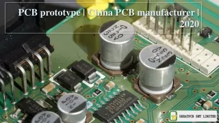
QC on PCBs • Besides systematic dimension deviations local defects on the PCBs are a QC issue: Repaired lines are straight, width variations are small Defect: Interconnected strips Damaged strip, huge width variation Strip is broken dead channel Joerg Wotschack
Considerations for the discussion • Tracks from the IP have inclinations between 7 and 35 degrees • Typical cluster sizes (track projection onto readout strips) are 10 – 28 mm or 3(4) to 8(10) strips. • A missing or interconnected strip will lead to a missing or wrong strip signal and thus to a larger position error • Comparable effects are created by the pillars (1% inefficiency) • Proposal: accept defects at a similar level as the inefficiency created by the pillars • ≤10 interconnected lines (shorts) as long as they are distributed; minimum distance between defects: 10 strips • ≤ 10 interrupted lines/PCB (1024 channels) as long as they are distributed; minimum distance between defects: 10 strips • The sum of interconnects and shorts: ≤10/PCB; minimum distance between defects: 10 strips Joerg Wotschack
What about spares? • How many PCBs of each type do we want to order? Minimum is 64 PCBs of each type • To cope with defects • To allow for selection of PCBs • To allow for accidents during panel construction • Is it cheaper to accept defects and to produce 10–20% more boards? • Option on re-processing after full delivery Joerg Wotschack
Test glueingstatus • End of last year we decided to ask industry for tests for Kapton foil glueing and pillar deposition over the (almost) full size PCBs (0.5 x 2.16 m) • Labs agreed to take responsibility for getting these tests done • Saclay deals with ELVIA • Frascati with ELTOS • US with Triangle Lab (tbc) • Goal is to have results by beginning of May Joerg Wotschack
Next steps • PCB layout version 0 exists (Givi) • Try to get agreement on general features today • Next steps • Integration with mechanics and FE board layout (AZ) and possibly other electronics boards until 15 April • Final checks with PCB lab until end April • Drawings ready for Module-0 ordering by 1 May • Need to order ≈100 PCBs for Module-0s • Order in three industries (ELTOS, ELVIA, Triangle Lab) ? Joerg Wotschack