Download
1 / 18
180 likes | 344 Vues
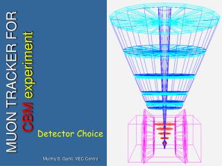
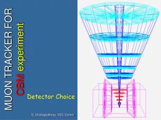
MC of CBM Silicon Tracker Status Report. Valeri Saveliev Obninsk State University, Russia 10.05.2004 GSI, Darmstadt. CBM Spectrometer and Silicon Tracker (STS). STS: Station z Rmin Rmax [cm] [cm] [cm] 1 5 0.5 2.5 2 10 0.5 5.0 3 20 1.0 10.0 4 30 1.5 15.0 5 40 2.0 20.0

E N D
MC of CBM Silicon TrackerStatus Report Valeri Saveliev Obninsk State University, Russia 10.05.2004 GSI, Darmstadt V.Saveliev
CBM Spectrometer and Silicon Tracker (STS) STS: Station z Rmin Rmax [cm] [cm] [cm] 1 5 0.5 2.5 2 10 0.5 5.0 3 20 1.0 10.0 4 30 1.5 15.0 5 40 2.0 20.0 6 80 4.0 40.0 7 100 5.0 50.0 Run Conditions: BX 10 MHz • STS: • Momentum measurement (Mag. Field); • Primary Vertex Reconstruction; • Secondary Vertex Recionstruction; V.Saveliev
MC of CBM Si Tracker Moscow State University – Si Technology and Production, Moscow Engineering and Physics Institute (University): Front-End Electronics; Obninsk State University: MC and Analysis; St. Petersburg KRI, SKBM: Support Design and Construction. Monte Carlo: Obninsk State University: V.Saveliev, PhD student D.Rizjikov, A.Golovin, Student O.Stotski St. Petersburg : V.Kondratiev V.Saveliev
Monte Carlo of CBM Silicon Tracker • VMC CBM Simulation Framework – is Good Step for Starting. • Simulation Environment for STS: • Accounts and Connections to GSI is established from Obninsk and St. Petersburg; • Local Version of CBM VMC has been installed in Obninsk Uni on Linux Cluster ( CPU time is ~10 Min for full simulation of Au+Au event 25 AGeV ); V.Saveliev
MC of CBM G4 version of VMC CBM Central Au+Au at 25 AGeV V.Saveliev
MC of STS CBM Event 1, Proj. (197,79), Targ (179,79), E= 25 GeV/u, Track 1641 / 1641 STS detector sts_station_1: 505 Hits STS detector sts_station_2: 677 Hits STS detector sts_station_3: 706 Hits STS detector sts_station_4: 721 Hits STS detector sts_station_5: 720 Hits STS detector sts_station_6: 706 Hits STS detector sts_station_7: 699 Hits V.Saveliev
Si-Strip Sensors with Stereo Angles Simplest solution for technology: Double Side Si Strip Detectors with Stereo angles on single wafer Implemented in G4 CBM Geometry V.Saveliev
STS Sensors versions: Rf Implemented in G4 CBM Geometry V.Saveliev
STS Sensors versions LL Long Ladder Si Strip Detectors (Si LC Project) V.Saveliev
Occupancy of Silicon Tracker Hits density (central Au+Au at 25 AGeV) in STS V.Saveliev
Segmentation of Silicon Strip Tracker Occupancy 1%; 5% ------------------------------------------------------------- Strip Pitch 25 mm; 12.5 mm ------------------------------------------------------------- Strip Length 0.4 mm 4 mm Analysis in progress Hits density of Station1 of STS (central Au+Au at 25 AGeV) V.Saveliev
Thickness of Si-Strip Tracker Sensors Multiple Scattering is limitations: Study is in progress: Thickness of Si Sensors is in the range 100 – 300 mkm V.Saveliev
Radiation Environment ? V.Saveliev
Radiation Environment ? GaAs:Cr for HEP - radiation testsYu Arestov (IHEP) IHEP, Protvino NCPHEP, Minsk SIPT, Tomsk ICBP, Puschino V.Saveliev
Doping GaAs by Chromiumthe 5-year practice of a new technology in Tomsk • World studies of GaAs irradiation tolerance related mainly to GaAs structures of the previous generation. • A new unique production technology of GaAs:Cr (doped by Chromium) belongs to Tomsk. • As was earlier shown by estimates and by the first measurements (Protvino, RAL), GaAs:Cr radiation hardness can be higher than that of Si by a factor of 10 or larger. V.Saveliev
More Detailed Analysis of STS Station3: St Petersburg V.Kondratiev V.Saveliev
More Detailed Analysis of Station3: St Petersburg V.Kondratiev V.Saveliev
Next Steps: The Tool for Monte Carlo Simulation is exist • Position Resolution of Si Strip Detectors and Segmentation fits to CBM Requirements. • Geometrical Layout of Si-Strip Stations of STS. • Support Design and Implementation. • Radiation Environment Analysis. • Hits Structure, • Digitalization, • Connection to the Reconstruction Chain, • Optimization of Si-Strip Station of STS for the physics of CBM Open Charm and Low Mass Vector Mesons. V.Saveliev