Overview of CNR-IFSI PACS Data Processing Unit Block Diagram and Component Breakdown
This document provides a detailed overview of the CNR-IFSI PACS Data Processing Unit (DPU) block diagram, showcasing the interconnections between sub-systems including SWL detectors, control interfaces, and communication links. It also presents a comprehensive mass breakdown of key components such as CPU boards, DC/DC converters, and interface boards, offering insights into their weights and specifications. Additionally, the document outlines high-speed serial links for data exchange, essential for system operation and telemetry, ensuring efficient communication and integration within the PACS architecture.

Overview of CNR-IFSI PACS Data Processing Unit Block Diagram and Component Breakdown
E N D
Presentation Transcript
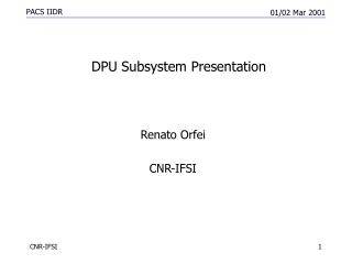
DPU Subsystem Presentation Renato Orfei CNR-IFSI CNR-IFSI
General Block Diagram PACS S/S SWL DET. GRATING ASS. CHOPPER ASS. FLIP MIRROR ASS. LWL DET. MEC 1 MECH-CONTROL1 SWL DETECTOR CONTROL DPU-OM SPU-NOM S/C DPU-RED SPU-RED MEC 2 MECH-CONTRO 2 LWL DETECTOR CONTROL CNR-IFSI
Data RAM TWO Serial I/F To/From SPU 512 Kw2 MB Data area32 bit words EEPROM Inst. Program 262 Kw1 MB ICU TSC 21020 DSP ONE Serial I/F To/From DEC/MEC FPGA State Machine PROM Kernel Telemetry upload SW 5.4 Kw32 KB Program RAM Instr. Program From EEPROM Program area48 bit words 512 Kw3 MB S/C DPU General Block Diagram CNR-IFSI
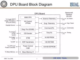
DPU High level block diagram CNR-IFSI
CPU Block Diagram CNR-IFSI
DC/DC Converter Block Diagram CNR-IFSI
DPU Mass breakdown • Components of the mass breakdown:BOX (240x258x194 mm^3, thickness 3 mm, 2.7 g/cm^3): Baseplate 240x258x3= > 501.5 g Front wall: 240x194x3=> 377.1 g Front wall connectors (delta:E)=> 150 g Bak wall: 240x194x3=> 377.1 g Lateral walls: 258x194x3x2=> 754.3 g Cover: 240x258x3=> 501.5 g Total Box weight: 2661.5 g • CPU boards: 2x 600 g => 1200 g • P/L I/F Boards: 2x 480 g => 960 g • DC/DC boards: 1000 g => 1000 g • Motherboard: 400 g => 400 g • Screws etc.: 100 g => 100 g • Cabling: 300 g => 300 g Total estimated weight: 6621.5 g (+ - 10 %) CNR-IFSI
CDMS COMMUNICATION I/F CNR-IFSI
CDMS Event Pkt CPU POWER SUPPLY I/F 28 V lines S/C operated plus synchronization from S/C to PACS: • One I/F for DPU DC/DC converter • Other I/Fs for SPU and DEC/MEC controlled by DPU via “Event Pkt” S/C DPU SPU & DEC/MEC DC/DC DC/DC 28Vswitches CNR-IFSI
Subsystems Interfaces All HW interfaces implemented with balanced drivers and receivers (LVDS) • 3 high speed serial bi-directional links for science data and HK collection: - 2 links to/from SPU-1 link to/from DEC/MEC • The links will be used for subsystems commanding and reception of science and HK data CNR-IFSI
S/C Interface Block diagram CNR-IFSI