
Low-Power Offset Correction Circuit Design for Filters
E N D
Presentation Transcript
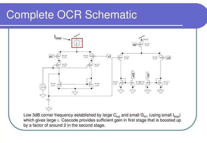
M=0.25 I=0.16nA vb W='10*l' L='10*l' vrf W='10*l' W='10*l' v1 W='10*l' W='10*l' vrf L='10*l' L='10*l' L='10*l' L='10*l' W='10*l' W='10*l' L='10*l' L='10*l' voll vor W='10*l' W='10*l' W='10*l' W='10*l' W='10*l' W='10*l' L='10*l' L='10*l' L='10*l' L='10*l' L='10*l' L='10*l' V=1.05 C=10pF Complete OCR Schematic Ibias Low 3dB corner frequency established by large Cout and small Gm1 (using small Ibias) which gives large t. Cascode provides sufficient gain in first stage that is boosted up by a factor of around 2 in the second stage.
Circuit Block Diagram The DC gain of the offset correction circuit is set by Gm1*Ro and the corner frequency is set by Gm1*Cout. Gm2 is the V-to-I conversion to allow a current feedback into the original filter OTA.
Simulation3-f-offset-ac Simulation3-f-offset-ac vm(out) vm(out) vm(x) vm(x) 1 1 100m Voltage Magnitude (V) 100m Voltage Magnitude (V) 10m 10m 1m 1m 100u 100u 100m 1 10 100 1k 10k 100k 1M 100m 1 10 100 1k 10k 100k 1M Frequency (Hz) Frequency (Hz) AC Response Verification Q=2; f90=300Hz Q=2; f90=2kHz
Simulation3-f-offset v(out) 1.70 v(x) 1.65 1.60 Voltage (V) 1.55 1.50 1.45 1.40 0.50 0.55 0.60 0.65 Time (s) Stability Verification
Simulation3-f-offset-dc Simulation3-f-offset (1.61, 1.58) (1.51, 1.58) dx=104.00m dy=200.00u v(out) v(out) 1.75 v(x) v(x) 1.70 1.5 Voltage (V) Voltage (V) 1.65 1.0 1.60 1.55 0.5 1.50 0.0 1.30 0.0 1.35 0.1 1.40 0.2 1.45 0.3 1.50 0.4 1.55 1.60 0.5 1.65 0.6 1.70 0.7 1.75 0.8 1.80 0.9 1.85 1.90 1.0 Time (s) vdc (V) DC Behavior and Startup Time DC behavior of OCR Startup time verification
Final Results • Q=2, f90=10kHz filter uses 6.13mW (bonus) • f90 variable from 100Hz to 10kHz; Q variable from 1 to 6 • Effective noise sources N=4.81, VL=0.765V which results in DR > 60dB • Filter attenuation at HF past f90 = -75dB; < 1dB variation from unity gain in passband • Power to correct 10kHz filter = 480.48nW • Power-on startup time = 0.12s (bonus) • 14 transistors used for OCR circuit (bonus) • Maximum cap size = 10pF • Lowest current used = 0.16nA • Entire layout fits in ¼ of padring area (bonus)