Comprehensive Overview of 4-Bit Multiplexers and ALU Design Principles
This document provides a detailed analysis of 4-bit multiplexers, ALU operations, and memory management within digital systems. It covers the functionality of multiplexers in selecting inputs based on control signals, the design of arithmetic logic units (ALUs) with various operation codes, and the fundamentals of general-purpose shift units for data manipulation. The report emphasizes the importance of registers, decoding write addresses, and the control of memory operations. It serves as a detailed review for designing complex digital systems effectively.

Comprehensive Overview of 4-Bit Multiplexers and ALU Design Principles
E N D
Presentation Transcript
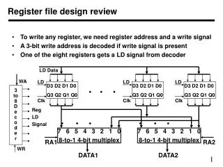
LD Data WA 3 to 8 D e c o d e r Reg LD Signal LD LD LD D3 D2 D1 D0 D3 D2 D1 D0 D3 D2 D1 D0 7 6 5 4 3 2 1 0 8-to-1 4-bit multiplex 7 6 5 4 3 2 1 0 8-to-1 4-bit multiplex Q3 Q2 Q1 Q0 Q3 Q2 Q1 Q0 Q3 Q2 Q1 Q0 RA1 RA2 Clk Clk Clk DATA1 DATA2 WR Register file design review • To write any register, we need register address and a write signal • A 3-bit write address is decoded if write signal is present • One of the eight registers gets a LD signal from decoder
0 1 2 3 MUX MUX MUX Add/sub Result A A OR ADD/SUB B B 0 1 A A 0 AND MUX B 1 B Sel0 Sel0 Sel0 Sel2 Sel1 An eight function ALU design review • ALU operation code and their meanings are • 000 Output A 100 A + B • 001 Output B 101 A - B • 010 Output 00..0 110 A and B • 011 Output 11..1 111 A or B • Three bits are Sel2, Sel1, and Sel0 • Sel0 makes first set of groups • Selects one of the two functions • Sel2 and Sel1 selects final output • It is one of the four groups
D3 D2 D1 D0 Q3 Q2 Q1 Q0 4-to-1 Mux 4-to-1 Mux 4-to-1 Mux 4-to-1 Mux D3 D2 D1 D0 SC Q3 Q2 Q1 Q0 D D D D Q Q Q Q Q3 Q2 Q1 Q0 Clock C C C C Clock Shifter unit review • A general-purpose shift unit controls load input of the register • Shift operation is controlled by two bits SC (s1 s0) as follows • 00 No change in register 10 Shift left • 01 Load new data 11 Shift right • Thus a flip flop at position i gets its own value Qi, a new external value Di, a value on its right Qi-1, or a value on its left Qi+1 • A 4-to-1 multiplexer at the input of each flip flop is thus needed • For non-registered data shift unit we only need multiplexers
RAM Addr Data out Data in Read Write Memory unit • A general-purpose memory has M words • M is generally a power of 2 (like 2, 4, 8, …, 1024, .., 2m) • Each word is n-bit wide • An m-bit address specifies which word is to be written or read • A read and a write signal control read and write operations • Some memories are read only (ROM), they are written once or more times using various mechanisms • A read/write memory using any address is called RAM
ek e1 e0 A bus structure review • There are more than one source of data on a set of wire (bus) • We have enable signals to decide who will write on bus • The data from bus can be written into more than one units • Data are n-bit wide, n depends on data bus width • The value of k depends on number of sources • Only one source should be enabled on bus • We need multiplexing, typically achieved by tri-state buffers • An example bus is shown below
RA1 RA2 Input Output M- Reg LDM WOUT OpCode Reg File EMR EALU EI A L U S H I F T WM Mem Unit RM WR SC WA Addr EM WAD Now we are ready to write control • Using the data path design, we can carry out meaningful ops • Add two registers and write results in any register • Transfer memory data into registers, output • Transfer register data into memory, output