Register Cell Design
Register Cell Design. Large System architecture. Large digital systems typically partitioned into: Datapath Many registers, lots of Combinational Logic Moves / processes system data Operation specified by control word (from CU) Control Unit Many states and inputs

Register Cell Design
E N D
Presentation Transcript
Large System architecture • Large digital systems typically partitioned into: • Datapath • Many registers, lots of Combinational Logic • Moves / processes system data • Operation specified by control word (from CU) • Control Unit • Many states and inputs • Specifies what DP does next • Decisions made based on DP status information
Large System Block Diagram Control Inputs Control Unit Datapath Data Outputs Control Control Outputs Status Data Inputs
Register Transfer • The movement of data stored in registers and the processing performed on the data are referred to as Register Transfer Operations • Register Transfer Language (RTL) captures register transfers and it’s components of: • The registers within the system • The operations performed on system data • The control that defines the sequence of operations
Microoperations • Each register has a set of elementary operations it can do • E.G. Load, Increment, Shift, etc. • The combination of elementary register ops and combinational functions define simple system operations • These are the Microoperations of the system • Usually performed in a single clock cycle • Sequence of -ops specified by control unit
Register Transfer Notation • Register transfer source information may be • A single source register • External input data • Results of combinational logic operation • E.G. R0 R1 IR M[AR] (memory read at loc AR) PC PC + 1
Multiplexer-based Transfer • You have a limited number of local data sources E.G. K1: R1 R3 K2: R1 R1 + R2 Two sources are defined; use a 2 to 1 mux Small combinational function need to translate the K1 and K2 controls to the mux select and register load control signals
Multiplexer-based Register Transfer General Circuit Pattern Dest. Reg. MUX Src 1 Src 2 EN Src n Clk select Comb. Logic Controls
Multiple Register Transfers with MUXes • Systems usually have multiple destination registers, each with multiple sources • Common to have multiple reg. transfers at the same time • Designer has some choice of implementation • Use separate multiplexer for each destination • Use a shared multiplexer for all dest. Registers • Perform the source selection function with three-state outputs
Dedicated Multiplexers REGB MUX Reg. A Advantage is multiple register transfers can take place at the same time. REGC REGD SELA LDA REGA MUX Reg. B REGC REGD SELB LDB REGA MUX Reg. C REGB REGD Disadvantage is lots of hardware is needed. SELC LDC REGA MUX Reg. D REGB REGC SELD LDD Clock
Shared Multiplexer Reg. A Advantage is less hardware is needed. LDA Reg. B REGA MUX REGB LDB REGC REGD Reg. C Disadvantage is only one register transfer source can be selected at a time. SEL LDC Reg. D LDD Clock
Selection via Three State Outputs Reg. A ENA LDA Now the sources can be distributed; only the three state bus needs to go from source to source Only one source can be selected at a time but much less wire is needed. Reg. B ENB LDB Reg. C ENC LDC Reg. D END LDD Clock
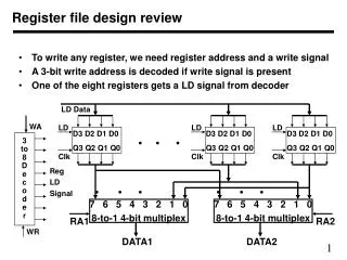
Register Cell design • Design the input of a register’s individual cell with several inputs with different control signals • Repeat it for n cells. Example: Design the register cell Ai with the following microoperations are to be performed on register A: SHL: A shl A EXOR: A A exor B ADD: A A+B
Register Cell design Assume only one of control signals SHL, EXOR and ADD is 1 at a time. If all zero ‘No Change’. Also we have a parallel adder available.Even though more complicated designs are available as in your book, direct application of combinational circuit- multiplexer comb. is the preferred method.
Register Cell design Si Ai EXOR Bi Ai-1 4x1 mux Ai D Load Select ADD EXOR SHL Comb. Logic Note: Design the combinational logic yourselves.
Register Cell design • Use a register with parallel loadwith D FF’s • Load= SHL+EXOR+ADD • Di= EXOR(Ai exor Bi)+SHL( Ai-1)+ADD (Ai exor Bi exor Ci) • Ci+1=(Ai+Bi)Ci+AiBi