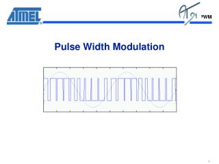
Pulse Width Modulation (PWM) LED Dimmer Circuit
Pulse Width Modulation (PWM) LED Dimmer Circuit. Using a 555 Timer Chip. Goals of Experiment. Demonstrate the operation of a simple PWM circuit that can be used to adjust the intensity of a green LED by varying the value of one resistor.


Pulse Width Modulation (PWM) LED Dimmer Circuit
E N D
Presentation Transcript
Pulse Width Modulation (PWM) LED Dimmer Circuit Using a 555 Timer Chip
Goals of Experiment • Demonstrate the operation of a simple PWM circuit that can be used to adjust the intensity of a green LED by varying the value of one resistor. • Demonstrate how a square wave generator can be built using an operational amplifier. • Demonstrate how a summing amplifier can be used to add a dc offset to a time-varying signal. • Describe how to test complex circuits.
Pulse Width Modulation An energy efficient technique that is used widely in industrial and consumer electronics to vary the power dissipated by a load. • Electric motors • Electric stove elements • Light dimmers
How a 555 Timer Works • Astable Multivibrator Mode http://www.williamson-labs.com/480_555.htm
Voltage Comparator • Op Amp circuit without a feedback component. • Output voltage changes to force the negative input voltage to equal the positive input voltage. • Maximum value of the output voltage, Vo, is V+ if the negative input voltage, v1, is less than the positive input voltage, v2. • Minimum value of the output voltage, Vo, is V- if the negative input voltage, v1, is greater than the positive input voltage, v2.
Transistor • As you will learn in ECE 2204, a transistor can be designed to act like a switch. • When a positive voltage is applied to the base of the transistor (B), the transistor acts like there is a very small resistor is between the collector (C) and the emitter (E). • When ground is applied to the base of the transistor (B), the transistor acts like there is a an open circuit between the collector (C) and the emitter (E).
Monostable Multivibrator • The frequency of the output from the 555 timer is constant. It is determined by the RC time constant of the external components, Ra and C1, and the frequency of the voltage source tied to the Trigger input pin. • The width of the 5V pulse within a cycle is determined by the amplitude of the signal on the Control pin of the 555 Timer chip.
PWM Voltage on Control pin Output voltage of the 555 Timer http://www.hobbyprojects.com/general_theory/pulse_modulation.html
Square Wave Generator:Relaxation Oscillator The duty cycle of the output will be 50% when R1 = R2. The frequency of the square wave output is given by:
The delay in obtaining the square wave output is a result of • the initial condition of the capacitor (IC = 0V), • the amount of electronic noise in the circuit, • the degree to which your op amp is nonideal, and • the RC time constant of the charging circuit for the capacitor.
Square Wave with Offset Voltage Vo 0-5V square wave
Light Emitting Diode (LED) • A nonlinear component that ‘looks’ like a battery when it is on and an open when it is off.
Anode vs. Cathode • Switch your DMM to the diode symbol. • Place the red probe into the V-W plug and the black probe into the COM plug. • Place your probes across the diode. • If the result is a very small number, then your red probe is contacting the anode and the black probe is contacting the cathode of the diode. • If the result is an overload (overflow) condition, then the red probe is contacting the cathode and the black probe is contacting the anode of the diode.
Simulating a LED in PSpice No LED part in the student PSpice so we use a series combination of parts. • Dbreak (diode breakout part) • Allows current to flow when the voltage on the anode is 0.7V higher than the voltage on the cathode. • Vdc • Set to the difference in the voltage needed on the anode to turn the LED on • Our red and green LEDs need between 2-2.5V.
Experimental Procedure • First, construct and test the square wave generator. • Second, construct and test the summing amplifier circuit. • Only after verifying that the two circuits operate correctly, connect them together. • Third, construct the pulse width modulator circuit using the 555 timer. • If the circuit doesn’t work properly, rework the circuit as a monostable vibrator and connect the Velleman function generator (500 Hz square wave with a peak-to-peak voltage of 5V and an offset voltage of 2.5V) to the trigger.
Debugging • Find reasonably points within circuit to make measurements. • Start at the beginning of the circuit: • Compare measured voltages with expected voltages obtained either through circuit analysis or simulation. • This means that you should do your calculations and simulations before you construct the circuit. • If they match reasonably well, move on to the next measurement point.
If they don’t, do the simple things first: • Verify that power is on and connected at the right places (particularly V+ and V- on op amps). • Check component values. • Run through wiring to make sure that the wires are going where they are supposed to and nothing is accidently touching. • Make sure that your oscilloscope probes are connected to the correct points in the circuit. • Replace Rf on the summing amplifier if the output voltage is not close of a 0V-5V square wave. • The circuit usually works even if the max. of the output voltage is 3.5V instead of 5V. • Only if you are confident that you have everything above right, consider replacing the op amp or 555 timer chip. • If the circuit still doesn’t function properly, see one of the OpEL GTA for assistance.
Pre-Lab • This is a longer lab so the answers for the questions in the Analysis Section are: RLED = 2.5V/10mA = 250 W. f = 1/[2ln(3)(910 W)(1mF)] = 500Hz Vopamp2= -(1k W /3.6k W) Vsqwave -(1k W /3.6k W)(-9V Vopamp2= -0.278 Vsqwave + 2.5V • You must enter the results from the PSpice simulations described in the experimental procedure (and on the next slide).
Pre-Lab Report 1. The plot generated from the transient analysis of the circuit in Figure 1 using: • a 10 kΩ resistor instead of the trim pot for Ra • V2 is a sinusoidal input voltage source with amplitude of 2V with a 2V offset voltage and a frequency of 60Hz. • Vpulse should have a magnitude of 5V and a period of 200us with a 50% duty cycle. • V2 and V3, are displayed as well as the output voltage. The final time for the transient analysis should be 50 ms. 2. The plot generated from the transient analysis of the circuit in Figure 1 where the value of Ra is changed to 1 kΩ. 3. The plot generated from the transient analysis of the circuit in Figure 1 where the value of Ra is changed to 100 Ω. 4. The plot generated from the transient analysis of the circuit in Figure 2 where the value of Ra is changed to 1 kΩ where voltage probes are placed atthe output pin of both operational amplifiers. The final time for the transient analysis should be 40 ms.
Post-Validation Report • See the description of items to be include in the Instructions for LED Dimmer