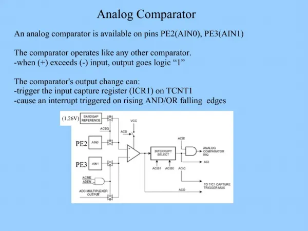
CMOS Comparator
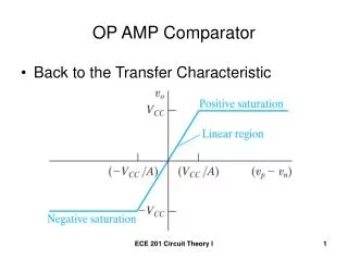
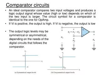
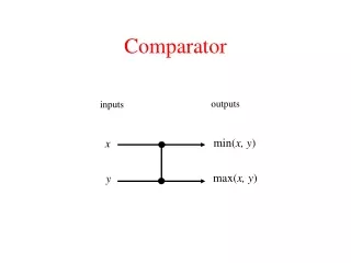
CMOS Comparator. Comparator. Transfer characteristic (ideal). Circuit symbol. Detects the polarity of the analog input signal and produces a digital output (1 or 0) accordingly – threshold-crossing detector. Applications. Voltage/current level comparison (A/D conversion)


CMOS Comparator
E N D
Presentation Transcript
Comparator Transfer characteristic (ideal) Circuit symbol Detects the polarity of the analog input signal and produces a digital output (1 or 0) accordingly – threshold-crossing detector
Applications • Voltage/current level comparison (A/D conversion) • Digital communication receivers (“slicer” or decision circuit) • Sense amplifier in memory readout circuits • Power electronics with digital control (dc-dc converter)
Design Considerations • Accuracy (offset, noise, resolution) • Settling time (tracking BW, regeneration speed) • Sensitivity (gain) • Metastability (any decision is better than no decision!) • Overdrive recovery (memory) • CMRR • Power consumption
Comparator Amplification Clipping • Precise gain and linearity are often unnecessary → simple, low-gain, open-loop, wideband amplifiers + latch (positive feedback) • More gain can be derived by cascading multiple gain stages • Built-in sampling function with latched comparators
Multi-Stage Preamp N stages:
Optimum N • Given A0 = Vo/Vi, Nopt can be determined with the above equation • For A0 < 100, typical N value ranges between 2 and 4
Comparison • A higher A0 (= Vo/Vi) requires a larger N • In comparison, latches regenerate faster than preamps
Multi-Stage PA Offset Individual stage Total input-referred
Input Offset Cancellation • AC coupling at input with input-referred offset stored in C • Two-phase operation, one phase (Φ2) is used to store offset
Offset Storage – Φ2 Closed-loop stability (amplifier in unity-gain feedback) Ref: J. L. McCreary and P. R. Gray, “All-MOS charge redistribution analog-to-digital conversion techniques. I,” JSSC, vol. 10, pp. 371-379, issue 6, 1975.
Amplifying Phase – Φ1 • Offset cancellation is incomplete if A is finite • Input AC coupling attenuates signal gain
CF and CI of Switches • What’s the optimum phase relationship between Φ2 and Φ2'? • Bottom-plate sampling → Φ2' switches off slightly before Φ2 (note the operation in this phase is signal independent anyway)
Output Offset Cancellation • AC coupling at output with offset stored in C • A must be small and well controlled (independent of Vo) • Does not work for high-gain op-amps
Offset Storage – Φ2 • Closed-loop stability is not required • CF and CI of Φ2' gets divided by A when referred to input Ref: R. Poujois and J. Borel, “A low drift fully integrated MOSFET operational amplifier,” JSSC, vol. 13, pp. 499-503, issue 4, 1978.
Amplifying Phase – Φ1 • Cancellation is complete if A is constant (independent of Vo) • AC coupling at output attenuates signal gain
Offset Cancellation w/ Auxiliary Input • Gm1 and Gm2 are the preamp and latch, respectively • A form of output offset cancellation technique Ref: B. Razavi and B. A. Wooley, “Design techniques for high-speed, high-resolution comparators,” JSSC, vol. 27, pp. 1916-1926, issue 12, 1992.
Offset Sampling • S3-S6 closed • S1-S2 open • Gm1 and Gm2 are grounded and the PFB of Gm2 is disabled • Vos1 and Vos2 are amplified by Gm1 and Gm2 to appear at Vo • When S5 & S6 open (slightly before S3 & S4), offset voltage is sampled and stored in C1 and C2 • CF/CI of S5 & S6 gets divided by (Gm1/Gm2) when referred to input
Comparison • S3-S6 open • S1-S2 closed • Differential input is amplified by Gm1 to establish an imbalance at the output and AC coupled to the input of Gm2 • Gm2 starts regeneration with this imbalance
Potential Problems • Very complicated → slow conversion speed • C1 and C2 and their parasitics add loading to the output • Finite on-resistance of S5 & S6 cannot completely break PFB • CF/CI imbalance of S5 & S6 can trigger regeneration
Razavi’s Comparator Even more complicated!
Overdrive Recovery Test “0” “1” Case I Case II A small input (±0.5 LSB) is applied to the comparator input in a cycle right after a full-scale input is applied; the comparator should be able to resolve to the right output in either case → memoryless
Passive Clamp • Limit the output swing with diode clamps → signal-dependent Ro • Clamps add parasitics to the PA output
Active Reset • Kill PA gain with a crowbar switch → time-dependent Ro • Switch adds parasitics to the PA output
PA Autozeroing • Two-phase operation, Φ2 phase is used for offset storage • Autozeroing switch Φ2' also resets and removes the PA memory
Pull-Up • NMOS pull-up suffers from body effect, affecting gain accuracy • PMOS pull-up is free from body effect, but subject to P/N mismatch • Gain accuracy is the worst for resistive pull-up as resistors (poly, diffusion, well, etc.) don’t track transistors; but it is fast!
To Obtain More Gain • Ip diverts current away from PMOS diodes (M3 & M4), reducing (W/L)3 • Higher gain w/o CMFB • Needs biasing for Ip • M3 & M4 may cut off for large Vin, resulting in a slow recovery
Bult’s Preamp • NMOS diff. pair loaded with PMOS diodes and PMOS latch (PFB) • High DM gain, low CM gain, good CMRR • Simple, no CMFB • (W/L)34 > (W/L)56 needs to be ensured for stability Ref: K. Bult and A. Buchwald, “An embedded 240-mW 10-b 50-MS/s CMOS ADC in 1-mm2,” JSSC, vol. 32, pp. 1887-1895, issue 12, 1997.
DM
CM
Song’s Preamp • NMOS diff. pair loaded with PMOS diodes and resistors • High DM gain, low CM gain, good CMRR • Simple, no CMFB • Gain not well-defined Ref: B.-S. Song et al., “A 1 V 6 b 50 MHz current-interpolating CMOS ADC,” in Symp.VLSI Circuits, 1999, pp. 79-80.
Song’s Preamp DM CM
Static Latch • Active pull-up and pull-down → full CMOS logic levels • Very fast! • Q+ and Q- are not well defined in reset mode (Φ = 1) • Large short-circuit current in reset mode • Zero DC current after full regeneration • Very noisy
Semi-Dynamic Latch • Diode divider disabled in reset mode → less short-circuit current • Pull-up not as fast • Q+ and Q- are still not well defined in reset mode (Φ = 1) • Zero DC current after full regeneration • Still very noisy
Current-Steering Latch • Constant current → very quite • Higher gain in tracking mode • Cannot produce full logic levels • Fast • Trip point of the inverters
Dynamic Latch • Zero DC current in reset mode • Q+ and Q- are both reset to “0” • Full logic level after regeneration • Slow Ref: A. Yukawa, “A CMOS 8-Bit High-Speed A/D Converter IC,” JSSC, vol. 20, pp. 775-779, issue 3, 1985.
Modified Dynamic Latch • Zero DC current in reset mode • Q+ and Q- are both reset to “0” • Full logic level after regeneration • Slow Ref: T. B. Cho and P. R. Gray, “A 10 b, 20 Msample/s, 35 mW pipeline A/D converter,” JSSC, vol. 30, pp. 166-172, issue 3, 1995.
Cho’s Comparator M1R and M2R added to set the comparator threshold