Download
1 / 17
170 likes | 325 Vues
Atomic Layer Deposition for SRF Cavities. Jeff Elam , Michael Pellin Jerry Moore*, Jim Norem Argonne National Laboratory Claire Antoine CEA Saclay/Fermi *also MassThink. SRF Materials Workshop FNAL, May 23-24, 2007. Outline. What is Atomic Layer Deposition (ALD)?

E N D
Atomic Layer Deposition for SRF Cavities Jeff Elam , Michael PellinJerry Moore*, Jim NoremArgonne National LaboratoryClaire AntoineCEA Saclay/Fermi*also MassThink SRF Materials Workshop FNAL, May 23-24, 2007
Outline • What is Atomic Layer Deposition (ALD)? • Why should ALD be considered for use in SRF cavities? • Near term ALD effort. • Replace the Niobia (NbxOy) layer inevitably present with an well defined, thin barrier layer. • Barrier layer should be • H diffusion barrier • O, N (H20, O2, etc.) diffusion barrier • Long term ALD effort. • Superconducting layer growth (Nb, NbN, Nb3Sn, MgB2, etc.) • Increase radius of curvature • Conclusions
Atomic Layer Deposition-What is it? • Atomic Layer by Layer Synthesis Method similar to MOCVD • Used Industrially • Semiconductor Manufacture for “high K” gate dielectrics • “Abrupt” oxide layer interfaces • Pinhole free at 1 nm film thicknesses • Conformal, flat films with precise thickness control • Electroluminescent displays • No line of sight requirement • Large area parallel deposition • Parallel film growth technique; Inside of large tubes can be done at once.
Ellipsometry Atomic Force Microscopy 4000 3500 3000 2500 Thickness (Å) 2000 1500 1000 Seagate, Stephen Ferro 500 0 • RMS Roughness = 4 Å (3000 Cycles) • ALD Films Flat, Pinhole free 0 500 1000 1500 2000 2500 3000 Flat, Pinhole-Free Film AB Cycles • Film growth is linear with AB Cycles ALD Reaction Scheme • ALD involves the use of a pair of reagents. • each reacts with the surface completely • each will not react with itself • This setup eliminates line of site requirments • Application of this AB Scheme • Reforms the surface • Adds precisely 1 monolayer • Pulsed Valves allow atomic layer precision in growth • Viscous flow (~1 torr) allows rapid growth • ~1 mm / 1-4 hours • No uniform line of sight requirement! • Errors do not accumulate with film thickness. • Fast! ( mm’s in 1-3 hrs ) and parallel • Pinholes seem to be removed. • Bulk
Apparatus • Hot wall reactor (RT-400 C) • Always coat the wall – now it will be useful
Oxide Nitride Element Ph/As C F S/Se/Te Demonstrated ALD A/B Reactions Element
Atomic Layer Deposition of Tungsten ( analogous to Nb synthesis using NbCl5 ) Overall Reaction: WF6 + Si2H6 → W + products • A) WSiHSiH3* + 2 WF6→ WWWF4* + 2 SiF4 + 3/2 H2 + HF • B1) WF4* + Si2H6 → WSiH2F* + SiHF3 + 3/2 H2 • B2) WSiH2F* + ½ Si2H6 → WSiHFSiH3* + 1/2H2 ALD W Binary Reaction Sequence: • ALD Growth Rate ~ 2 ML W per cycle • Small CVD component from Si2H6 thermal decomposition • Difficult to nucleate W ALD on many surfaces • W ALD nucleates well on Al2O3 → Deposit ALD Al2O3 “seed” layer F.H. Fabreguette et al, Thin Solid Films 488 (2005) 103 – 110. Grubbs et al, J. Vac. Sci. Technol. B 22(4) 1811.
ALD for SRF Cavities • ALD is an ideal tool for coating SRF cavities • Precision synthesis of ultra-thin films on complex surfaces • Films are adherent (growth mechanism requires it) • Films are pinhole free even at 1-2 nm film thicknesses (hence semiconductor industry’s choice of ALD for gate dielectric films) • Conformal coating -> reduced point radius of curvature • Alumina by ALD forms an extremely effective diffusion barrier to H, O, N etc. • TiN ALD reduces secondary electron surface yield and is a diffusion barrier. • With development ALD can grow the thin superconducting films necessary to enhance superconductor lower critical fields.
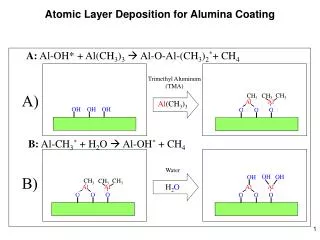
Near Term ALD Research – Replace poorly constrained Niobia with a more optimum dielectric Al2O3 capping layers for Nb surfaces • Surface behavior of Nb* • In air, Nb oxide layer • Annealed in vacuum • Al2O3 Capping Layer • 10 nm • Al(CH3)3 alternating H2O cycles • 20 C ->200 C deposition temperature • Anneal at 200 C to dissolve Niobia • Other caps? • TiN (Reduce Multipactering) *Ciovati, APL, 89 (2006) 022507/1-3 Delheusy, Antoine et al, thesis work
0 c 300 c 200 c 100 c 100 nm 400 c 500 c 600 c Conformal Coating Reduces Particulate Radius of Curvature • TiN coating or Alumina coating - residual particle effect might be reduced • Progressive growth of Ag nanoparticles with increasing number of Al2O3 cycles (c) • Ag nanoparticles still visible under 60 nm Al2O3 coating • AFM linescans show no net change in height → Al2O3 grows equally on Ag and SiO2
Where are we? • Nb coupons have been coated with alumina and TiN • Films are thin, pinhole free, adherent, • Coating reduces Nb Oxidation State • Initial TiN studies are encouraging. • We are working to coat a single cell cavity.
Higher-TcSC: NbN, Nb3Sn, etc Nb, Pb Insulating layers Long Term Goal of ALD SCRF • Build “nanolaminates” of superconducting materials • ~ 10- 30 nm layer thicknesses
What has been done. • Nanolaminates of Al2O3 and W • Growth conditions can set RMS roughness to < 0.4 nm • Higher temperature -> greater crystallinity
Proposal for bringing ALD to SCRF fabrication • Investigate the properties of Al2O3 capping layers for Nb surfaces • Al2O3 is the ALD “poster child” • Stabilize Nb surface oxides • Anneal to reduce oxide thickness • We are already using it to cap FePt particles (resist oxidation to 1000 C @ 10 nm thick film) • Synthesize Nb “bulk” layer on Al or Cu cavities • Develop the chemistries for “clean” deposition and crystallite control • In situ capping • Grow NbN, Nb3Sn, MgB2 layers on the Al2O3 capped Nb • Develop the chemistries for “clean” deposition and crystallite control • Test for enhanced field behavior • Scale-up • ALD was made for growing films on the inside of tubes – precision layer by layer growth at aspect ratios exceeding 10000 • Coating is of all surfaces, no field penetration at the corners or edges
Synthesize Nb “bulk” layer on Al or Cu cavities • Why? • Limit amounts of Nb needed • Single apparatus for Nb and cap layer – oxygen control • Reactions not demonstrated • NbCl5 + Si2H6 → Nb + SiCl4 + HCl • Analogous to W reactions with similar enthalpies • Precursors are volatile, stable, and purchasable at high purity • Challenges • Control of impurities (Cl) • Control of crystallite size (may require high temperature flash)
Atomic Layer Deposition of NbN Overall Reaction (T = 400 C): 3NbCl5 + 5NH3 → 3NbN + N2 + 15 HCl • ALD Growth Rate ~ 0.03 nm/cycle NbN per cycle • NbN ALD nucleates well on Al2O3 or SiO2 • Need to find synthesis conditions for “clean”deposition • Need to control crystallinity Higher-TcSC: NbN Nb, Pb Van Hoornick et al, Journal of the Electrochemical Society 153 (2006) G437. Alén et al, Thin Solid Films 491(1-2) (2005) 235. Insulating layers
Conclusions ALD to SCRF fabrication • ALD is an intriguing synthesis technique with many advantages for scrf cavities • Conformal coating means reduced radius of curvature • Parallel (non-line of sight) method • Flat samples directly map to complex shape samples even with high aspect ratios • Layer by layer growth on complex shapes • Clean path from caps to layered structures with much higher field gradients