Effect of Placement on Computational Memory Interface
130 likes | 246 Vues
Effect of Placement on Computational Memory Interface. Richa Prasad UMass, Distributed Mentoring Program, Intern Professor Elaheh Bozorgzadeh UCI, Distributed Mentoring Program, Mentor. Outline. Introduction Project Description Statement of Problem Purpose of Study Methodology

Effect of Placement on Computational Memory Interface
E N D
Presentation Transcript
Effect of Placement on Computational Memory Interface Richa Prasad UMass, Distributed Mentoring Program, Intern Professor Elaheh Bozorgzadeh UCI, Distributed Mentoring Program, Mentor
Outline • Introduction • Project Description • Statement of Problem • Purpose of Study • Methodology • The Wrapper File • FPGA Chip Selection & Description • The Process • Findings & Discussion • Description of Findings • Possible Future Work • Summary Recap Previous + New
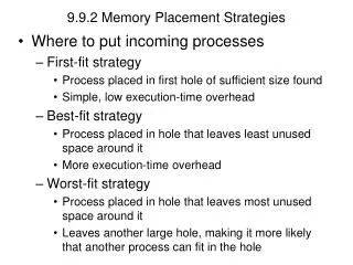
Recap… INTRODUCTION PROJECT DESCRIPTION DCM ASIC FPGA BRAM Chip Performance CLB Microprocessor Flexibility Multiplier Reset Enable Clock Data Wrapper File Synplicity Read Computational Block Synthesis User Constraint File Xilinx Project Navigator Write Memory Block Place & Routing Data Data Timing Report WRAPPER FILE PROCESS
…Recap FPGA DESCRIPTION WIRE TYPES • Farther locations – BRAM • Closer locations – CLB • CLB > BRAM as V500 to V8000 • CLB > BRAM as VP100 to VP20 • Frequency more for CLB CLB versus BRAM
New Observations… BRAM ACROSS CHIPS 7 4 1 8 5 2 6 3 • OBSERVATIONS • Doubled Frequency for V8000 & VP100 • Except V500, Frequency at 3 to 4 • VP100 Frequency > V8000 Frequency • Location 6 = 8 for all, except V500 • INFERENCES • Positioning important • V500 = small chip • Location 6 = 8 distance wise
…New Observations CLB ACROSS CHIPS 7 4 1 8 5 2 6 3 • OBSERVATIONS • Except at 7, V500, VP20, VP100 always • Frequency change than BRAM • V8000 & VP100 max change in frequency • Location 6 = 8, for V2000, V8000 & VP20 • INFERENCES • Positioning important more for CLB • More so for large chips • Location 6 = 8 distance wise
Delay Distribution across signal bits… LOCATION 1 – FARTHEST TOP Fail 1 • FAILED • Big change in distribution • High Standard Deviation • PASSED • Low Deviation • Most centered around mean Pass
…Delay Distribution across signal bits… LOCATION 3 – FARTHEST BOTTOM Fail • PASSED • Low Deviation • Delays centered around mean • All small delays use Long • FAILED • High Deviation • All small delays use Long 3 Pass
…Delay Distribution across signal bits… LOCATION 5 – MIDDLE MIDDLE Fail 5 Low Deviation, regardless of whether timing constraint is met or not Pass
…Delay Distribution across signal bits LOCATION 6 – MIDDLE BOTTOM Fail • FAILED • Low Deviation • 2 Fullhex wires used • PASSED • Low Deviation • Unihex most widely used 6 Pass
Possible Future Work • Switches met on each wire path • Change in wire type along each path • Redo experiments along with 1 and 2 on other chips
Summary • BRAM versus CLB an issue for larger chips • Farther locations – BRAM • Closer locations – CLB • CLB better choice on all chips for locations 6 to 8 • Positioning especially important for V8000 and VP100 • Overall frequency of V8000 < Overall frequency of VP100 • Memory block along farthest column of BRAM – Timing Failed – High delay distribution • Memory block along farthest column of BRAM – Timing Passed – Low delay distribution • Memory block along middle column of BRAM – Timing Passed/Failed - Low delay distribution

