Download
1 / 42
420 likes | 586 Vues
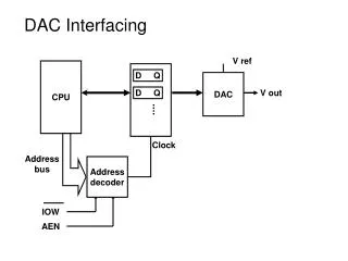
LHO 12 Interfacing. rd'/wr. Processor. Memory. enable. addr[0-11]. data[0-7]. bus. bus structure. A simple bus. Wires: Uni-directional or bi-directional One line may represent multiple wires Bus Set of wires with a single function Address bus, data bus

E N D
rd'/wr Processor Memory enable addr[0-11] data[0-7] bus bus structure A simple bus • Wires: • Uni-directional or bi-directional • One line may represent multiple wires • Bus • Set of wires with a single function • Address bus, data bus • Or, entire collection of wires • Address, data and control • Associated protocol: rules for communication
rd'/wr enable addr data tsetup tread read protocol rd'/wr enable addr data tsetup twrite write protocol Timing Diagrams • Most common method for describing a communication protocol • Time proceeds to the right on x-axis • Control signal: low or high • May be active low (e.g., go’, /go, or go_L) • Use terms assert (active) and deassert • Asserting go’ means go=0 • Data signal: not valid or valid • Protocol may have subprotocols • Called bus cycle, e.g., read and write • Each may be several clock cycles • Read example • rd’/wr set low,address placed on addr for at least tsetup time before enable asserted, enable triggers memory to place data on data wires by time tread
Microprocessor interfacing: I/O addressing • A microprocessor communicates with other devices using some of its pins • Port-based I/O (parallel I/O) • Processor has one or more N-bit ports • Processor’s software reads and writes a port just like a register • E.g., P0 = 0xFF; v = P1.2; -- P0 and P1 are 8-bit ports • Bus-based I/O • Processor has address, data and control ports that form a single bus • Communication protocol is built into the processor • A single instruction carries out the read or write protocol on the bus
Types of bus-based I/O: memory-mapped I/O and standard I/O • Processor talks to both memory and peripherals using same bus – two ways to talk to peripherals • Memory-mapped I/O • Peripheral registers occupy addresses in same address space as memory • e.g., Bus has 16-bit address • lower 32K addresses may correspond to memory • upper 32k addresses may correspond to peripherals • Standard I/O (I/O-mapped I/O) • Additional pin (M/IO) on bus indicates whether a memory or peripheral access • e.g., Bus has 16-bit address • all 64K addresses correspond to memory when M/IO set to 0 • all 64K addresses correspond to peripherals when M/IO set to 1
Memory-mapped I/O vs. Standard I/O • Memory-mapped I/O • Requires no special instructions • Assembly instructions involving memory like MOV and ADD work with peripherals as well • Standard I/O requires special instructions (e.g., IN, OUT) to move data between peripheral registers and memory • Standard I/O • No loss of memory addresses to peripherals • Simpler address decoding logic in peripherals possible • When number of peripherals much smaller than address space then high-order address bits can be ignored • smaller and/or faster comparators
Consider a simple processor. I call it the simple processing unit (SPU).
The memory read and I/O read timing for a simple processor is shown below.
The Memory write and I/O write timing for a simple processor is shown below.
Some Real processors No separate I/O address space.
Atmel AVR The 8051
8051 74373 HM6264 D<0...7> P0 Q D A<0...15> /CS /OE ALE G /WE CS2 /CS1 8 P2 /WR 27C256 /CS /RD D<0...7> /PSEN A<0...14> /OE Adr. 7..0 P0 P2 Q ALE /RD Data Adr. 15…8 Adr. 7…0 A basic memory protocol • Interfacing an 8051 to external memory • Ports P0 and P2 support port-based I/O when 8051 internal memory being used • Those ports serve as data/address buses when external memory is being used • 16-bit address and 8-bit data are time multiplexed; low 8-bits of address must therefore be latched with aid of ALE signal
8051 instructions for addressing external code and data memory.
8051 74373 HM6264 D<0...7> P0 Q D A<0...15> /CS /OE ALE G /WE CS2 /CS1 8 P2 /WR 27C256 /CS /RD D<0...7> /PSEN A<0...14> /OE Ex: XM(0) XM(1) CLR P2 CLR R0 MOV R1,#1 MOVX A,@R0 MOV R7,A MOVX A,@R1 MOVX @R0,A MOV A,R7 MOVX @R1,A Ex: XM(0) XM(1) MOV DPTR,#0 MOVX A,@DPTR INC DPTR MOV R7,A MOVX A,@DPTR XCH A,R7 MOVX @DPTR,A DEC DPTR XCH A,R7 MOVX @DPTR,A
RnC EQU P1.1 n_BUSY EQU P1.2 BYTE EQU P1.3
RnC EQU P1.1 n_BUSY EQU P1.2 BYTE EQU P1.3 CLR RnC SETB RnC JNB n_BUSY,$ MOV R7,P0 CPL BYTE MOV R6,P0
RESET_8255 EQU P1.0 CTL1 EQU 111111111011B ;ONE POSSIBLE ADDRESS FOR CONTROL PORT OF 8255 #1 PRTA1 EQU 111111111000B ;ONE POSSIBLE ADDRESS FOR PORT A OF 8255 #1 PRTB1 EQU 111111111001B ;ONE POSSIBLE ADDRESS FOR PORT A OF 8255 #1 PRTC1 EQU 111111111010B ;ONE POSSIBLE ADDRESS FOR PORT A OF 8255 #1 CTL2 EQU 111111110111B ;ONE POSSIBLE ADDRESS FOR CONTROL PORT OF 8255 #2 PRTA2 EQU 111111110100B ;ONE POSSIBLE ADDRESS FOR PORT A OF 8255 #2 PRTB2 EQU 111111110101B ;ONE POSSIBLE ADDRESS FOR PORT A OF 8255 #2 PRTC2 EQU 111111110110B ;ONE POSSIBLE ADDRESS FOR PORT A OF 8255 #2 CLR RESET_8255 ;REMOVE RESET FROM 8255 ;DO ADDITION C2|C1 <-- A2|A1 + B2|B1 MOV DPTR,#(CTL1 AND CTL2);POINT DPTR TO CONTROL REG OF 8255 #1 AND #2 MOV A,10010010B ;PRTA, PRTB IN, PRTC OUT MOVX @DPTR,A ;OUTPUT TO BOTH CONTROL REGS AT SAME TIME MOV DPTR,#PRTA1 ;SELECT PORT A OF 8255 #1 MOVX A,@DPTR ;GET PRTA1 MOV R7,A ;SAVE IT MOV DPTR,#PRTB1 ;SELECT PORT B OF 8255 #1 MOVX A,@DPTR ;READ PORT B OF 8255 #1 ADD A,R7 ;ADD PRTA1 TO PRTB1 MOV DPTR,#PRTC1 ;SELECT PORT C OF 8255 #1 MOVX @DPTR,A ;OUTPUT TO PRTC1 END
Figure 1. AT90S8515 with expanded memory. What should we do with A16? Answer: connect it to an unused port pin. Question: How could we map the entire 128K bytes of memory to the top 32 Kbytes of the AVR address space. Answer: Connect AVR A15 to /CE on U4. Now the memory is selected only when the AVR addresses the top have of the memory address space where A15 = 1. Connect A15 and A16 of U4 to unused AVR port pins. By changing these port pin, any of the four 32 K byte pages of U4 memory can be switched in and out of the AVR address space.