Download
1 / 42
570 likes | 1.27k Vues
Properties of Electrons, their Interactions with Matter and Applications in Electron Microscopy.

E N D
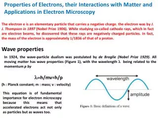
Properties of Electrons, their Interactions with Matter and Applications in Electron Microscopy The electron e is an elementary particle that carries a negative charge. the electron was by J. J. Thompson in 1897 (Nobel Prize 1906). While studying so-called cathode rays, which in fact are electron beams, he discovered that these rays are negatively charged particles. In fact, the mass of the electron is approximately 1/1836 of that of a proton. Wave properties In 1924, the wave-particle dualism was postulated by de Broglie (Nobel Prize 1929). All moving matter has wave properties (Figure 1), with the wavelength being related to the momentum p by h/mv=h/p (h : Planck constant; m : mass; v : velocity) This equation is of fundamental importance for electron microscopy because this means that accelerated electrons act not only as particles but as waves too.
An electron accelerated in an electric field V gains an energy E = eV which further corresponds to a kinetic energy Ekin = mv2/2. Thus: E = eV = m0v2 / 2 From this, the velocity v of the electron can be derived: v = (2eV/m)1/2 (V : acceleration voltage; e : electron charge = -1.602 176 487 × 10-19 C; m0 : rest mass of the electron = 9.109 x 10⁻³¹ kg). It follows for the momentum p of the electron: p(2meV)1/2 Now, the wavelength can be calculated from the de Broglie equation according to h/(2meV)1/2
The values calculated for acceleration potentials commonly used in TEM are listed in Table 1. It is important to note that these electrons move rather fast, and their speed approaches light velocity. As a result, a term considering relativistic effects must be added: (c : light velocity in vacuum = 2.998 x 10⁸ m/s). It thus is evident that relativistic effects cannot be neglected for electrons with an energy E ≥ 100 kV.
Characteristics of the electron wave Waves in beams of any kind can be either coherent or incoherent. Waves that have the same wavelength and are in phase with each other are designated as coherent. In phase with each other means that the wave maxima appear at the same site (Figure 2). The analogue in light optics is a Laser beam. On contrast, beams comprising waves that have different wavelengths like sun rays or are not in phase are called incoherent (Figure 2). Electrons accelerated to a selected energy have the same wavelength. Depending on the electron gun, the energy spread and as a result the wave length as well varies. Furthermore, the electron waves are only nearly in phase with each other in a thermoionic electron gun while the coherency is much higher if a field emitter is the electron source. The generation of a highly monochromatic and coherent electron beam is an important challenge in the design of modern electron microscopes. However, it is a good and valid approximation to regard the electron beam as a bundle of coherent waves before hitting a specimen. After interacting with a specimen, electron waves can form either incoherent or coherent beams.
Waves do interact with each other. By linear superposition, the amplitudes of the two waves are added up to form a new one. The interference of two waves with the same wavelength can result in two extreme cases (Figure 3): (i) Constructive interference: If the waves are completely in phase with each other, meaning that the maxima (and minima) are at the same position and have the same amplitude, then the amplitude of the resulting wave is twice that of the original ones. (ii) Destructive interference: If two waves with the same amplitude are exactly out of phase, meaning that the maximum of one wave is at the position of the minimum of the other, they are extinguished.
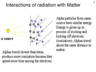
An electron passing through a solid may be scattered not at all once (single scattering) several times (plural scattering ), or very many times (multiple scattering ) Each scattering event might be elastic or inelastic. The scattered electron is most likely to be forward scattered but there is a small chance that it will be backscattered.
Electron-Matter Interactions Electron microscopy is not just a single technique but a diversity of different ones that offer unique possibilities to gain insights into structure, topology, morphology, and composition of a material. Various imaging and spectroscopic methods represent indispensable tools for the characterization of all kinds of specimens on an increasingly smaller size scale with the ultimate limit of a single atom. The wealth of very different information that is obtainable by various methods is caused by the multitude of signals that arise when an electron interacts with a specimen. Gaining a basic understanding of these interactions is an essential prerequisite before a comprehensive introduction into the electron microscopy methods can follow. A certain interaction of the incident electron with the sample is obviously necessary since without the generation of a signal no sample properties are measurable. The different types of electron scattering are of course the basis of most electron microscopy methods and will be introduced in the following.
When an electron hits onto a material, different interactions can occur, as summarized in Figure 4. For a systemization, the interactions can be classified into two different types, namely elastic and inelastic interactions. (i) Elastic Interactions In this case, no energy is transferred from the electron to the sample. As a result, the electron leaving the sample still has its original energy E0: Eel = E0 Of course, no energy is transferred if the electron passes the sample without any interaction at all. Such electrons contribute to the direct beam which contains the electrons that passes the sample in direction of the incident beam (Figure 4).
Furthermore, elastic scattering happens if the electron is deflected from its path by Coulomb interaction with the positive potential inside the electron cloud. By this, the primary electron loses no energy or – to be accurate – only a negligible amount of energy. These signals are mainly exploited in TEM and electron diffraction methods. (ii) Inelastic Interactions If energy is transferred from the incident electrons to the sample, then the electron energy of the electron after interaction with the sample is consequently reduced: Eel < E0 The energy transferred to the specimen can cause different signals such as X-rays, Auger or secondary electrons, plasmons, phonons, UV quanta or cathodoluminescence. Signals caused by inelastic electron-matter interactions are predominantly utilized in the methods of analytical electron microscopy.
Elastic Interactions Incoherent Scattering of Electrons at an Atom For the basic description of the elastic scattering of a single electron by an atom, it is sufficient to regard it as a negatively charged particle and neglect its wave properties. An electron penetrating into the electron cloud of an atom is attracted by the positive potential of the nucleus (electrostatic or Coulombic interaction), and its path is deflected towards the core as a result (Figure 5). The Coulombic force F is defined as: F = Q1Q2 / 4π εo r2 Smaller r, larger is F and consequently the scattering angle. In rare cases, even complete backscattering can occur, generating so-called back-scattered electrons (BSE). These electrostatic electron matter interactions can be treated as elastic, which means that no energy is transferred from the scattered electron to the atom. In general, the Coulombic interaction is quite strong, e.g. compared to that of X-rays with materials. Because of its dependence on the charge, the force F with which an atom attracts an electron is stronger for atoms containing more positives charges, i.e. more protons. Thus, the Coulomb force increases with increasing atomic number Z of the respective element.
Interaction cross-section and mean free path A cross section is the effective area which governs the probability of some scattering or absorption event The probability of scattering is described in terms of either an "interaction cross-section" or a mean free path. The concept of the interaction cross-section is based on the simple model of an effective area. If an electron passes within this area, an interaction will certainly occur. If the cross section of an atom is divided by the actual area, then a probability for an interaction event is obtained. Consequently, the likelihood for a definite interaction increases with increasing cross-section. Each scattering event might occur as elastic or as inelastic interaction. Consequently the total interaction cross section T is the sum of all elastic and inelastic terms: T =elastic + inelastic For every interaction, the cross section can be defined depending on the effective radius r:
For the case of elastic scattering, this radius relast is (Z : atomic number; e : elementary charge; V : electron potential; : scattering angle). This equation is important for understanding some fundamentals about image formation in several electron microscopy techniques. Since the cross-section and thus the likelihood of scattering events as well increases for larger radii, scattering is stronger for heavier atoms (with high) Z than for light elements. Moreover, it indicates that electrons scatter less at high voltage V and that scattering into high angles is rather unlikely. By considering that a sample contains a number of N atoms in a unit volume, a total scattering interaction cross section QT is given as
Introducing the sample thickness t results in This gives the likelihood of a scattering event. The term t is designated as mass-thickness. Inspite of being rather coarse approximations, these expressions for the interaction cross section describe basic properties of the interaction between electrons and matter reasonably well. Another important possibility to describe interactions is the mean free path , which unfortunately has usually the same symbol as the wavelength. Thus, we call it mfp here for clarity. For a scattering process, this is the average distance that is traveled by an electron between two scattering events. This means, for instance, that an electron in average interacts two times within the distance of 2mfp. The mean free path is related to the scattering cross section by:
For scattering events in the TEM, typical mean free paths are in the range of some tens of nm. For the probability p of scattering in a specimen of thickness t follows then:
TEMs are patterned after Transmission Light Microscopes and will yield similar information. Morphology The size, shape and arrangement of the particles which make up the specimen as well as their relationship to each other on the scale of atomic diameters. Crystallographic InformationThe arrangement of atoms in the specimen and their degree of order, detection of atomic-scale defects in areas a few nanometers in diameter. Compositional Information (if so equipped)The elements and compounds the sample is composed of and their relative ratios, in areas a few nanometers in diameter. In brief, a EM utilizes energetic electrons to provide morphologic, compositional and crystallographic information on samples.
The purpose of the C-lens is to focus the light onto the specimen. The condenser aperture controls the fraction of the beam which is allowed to hit the specimen.
1. The "Virtual Source" at the top represents the electron gun, producing a stream of monochromatic electrons. This stream is focused to a small, thin, coherent beam by the use of condenser lenses 1 and 2. The first lens (usually controlled by the "spot size knob") largely determines the "spot size"; the general size range of the final spot that strikes the sample. The second lens(usually controlled by the "intensity or brightness knob" actually changes the size of the spot on the sample; changing it from a wide dispersed spot to a pinpoint beam. 3. The beam is restricted by the condenser aperture (usually user selectable), knocking out high angle electrons (those far from the optic axis, the dotted line down the center). The beam strikes the specimen and parts of it are transmitted 4. This transmitted portion is focused by the objective lens into an image. Optional Objective and Selected Area metal apertures can restrict the beam; the Objective aperture enhancing contrast by blocking out high-angle diffracted electrons, the Selected Area aperture enabling the user to examine the periodic diffraction of electrons by ordered arrangements of atoms in the sample. 5. The image is passed down the column through the intermediate and projector lenses, being enlarged all the way. 6. The image strikes the phosphor image screen and light is generated, allowing the user to see the image. The darker areas of the image represent those areas of the sample that fewer electrons were transmitted through (they are thicker or denser). The lighter areas of the image represent those areas of the sample that more electrons were transmitted through (they are thinner or less dense).
TEM can be compared with a slide projector. In a slide projector light from a light source is made into a parallel beam by the condenser lens; this passes through the slide (object) and is then focused as an enlarged image onto the screen by the objective lens. In the electron microscope, the light source is replaced by an electron source, the glass lenses are replaced by magnetic lenses, and the projection screen is replaced by a fluorescent screen, which emits light when struck by electrons, or, more frequently in modern instruments, an electronic imaging device such as a CCD (charge-coupled device) camera. The whole trajectory from source to screen is under vacuum and the specimen (object) has to be very thin to allow the electrons to travel through it
Basic principle of Transmission Electron Microscope After having little knowledge that an accelerated electron beam can have a very high resolving power, we then move on to see how one can use this electron beam in imaging technology. There are 3 types of electron microscopes, namely the transmission electron microscope (TEM), scanning electron microscope (SEM), and scanning tunneling microscope (STM). In this Lecture we will introduce the basic principle of TEM. Fig. shows a schematic outline of a TEM. A TEM contains four parts: electron source, electromagnetic lens system, sample holder, and imaging system. A TEM functions under the same basic principles as an optical microscope.
Electron Gun…. At the top of the TEM column is the electron gun, which is the source of electrons. The electrons are accelerated to high energies (typically 100-400 keV) and then focused towards the sample by a set of condenser lenses and apertures. The electron beam comes from a filament, made of various types of materials. The most common is the Tungsten hairpin gun. This filament is a loop of tungsten which functions as the cathode. A voltage is applied to the loop, causing it to heat up. The anode, which is positive with respect to the filament, forms powerful attractive forces for electrons. This causes electrons to accelerate toward the anode. Some accelerate right by the anode and on down the column, to the sample. Other examples of filaments are Lanthanum Hexaboride filaments and field emission guns. Electron source of a TEM.
Selection of a Electron source or electron gun The source is chosen so that the rates of electrons incident on the sample per unit area and leaving the source per unit solid angle (brightness) are maximized. This is so that the maximum amount of information can be extracted from each feature of the sample. As I mentioned before there are two major types of electron source. Guns are more cheaper and more common of the to generate electrons by thermionic emission. If enough thermal energy is added to a material its electrons may overcome the energy barrier of the work function and escape. Unfortunately, to avoid the source melting, the material used must either have a very high melting point (such as W) or an exceptionally low work function (certain rare-earth boride crystals such as LaB6 are widely used). Another way of extracting electrons from a material is by applying a very large electric field. By drawing tungsten wire to a very fine point (<0.1 μm), application of a potential of 1 kV gives an electric field of 1010 A m-1which is large enough to allow electrons to tunnel out of the sample. This is called field emission. Field emission guns are around twice as expensive as thermionic electron guns, and must be used under ultra-high vacuum conditions. They are favorable for applications in which a high brightness and low energy-spread of incident electrons is needed. (e.g. HRTEM, FEG.)
.......................Electron Guns •Two main types of gun – Thermionic and Field Emission. •Thermionic sources produce electrons when heated. •Field emission sources produce electrons when exposed to an intense electric field. •FEG’s give much more brightness than thermionic systems. •FEG’s give a more monochromatic electron source and finer probe (i.e. better resolution). Comparison of the three types of source operating at 100kV
A thermionic electron gun is operated as follows: Select the accelerating potential ( kV ). Increase the current passing through the filament until the knee of the emission curve is reached (saturation), giving the best compromise between the beam current emitted (as high as possible) and the filament lifetime (as long as possible). Adjust the bias to give the desired combination of source size and beam current. J =AGT2 e-w/kT where J is the emission current density, T is the temperature of the metal, W is the work function of the metal, k is the Boltzmann constant, and AG is a parameter which is materials specific
Schottky and cold field-emission guns comparing in electron microscopes A field emission gun is based on a release of electrons from surface of sharply pointed tungsten tip as a result of application of a strong electric field (>107 Vm-1). The field emission is caused by applying a voltage between the tip and an aperture metal anode. There are two types of field emission gun differ mainly by their tips: CFE - cold field emitter is the base type. Application of the very strong electric field causes the surface energy barrier to deform to such an extent that it becomes physically very narrow. There becomes a finite probability of electrons from the Fermi level penetrating the barrier even at ambient temperature. Usually made of single crystal tungsten sharpened tip with radius of about 100 nm, the needle is so sharp that electrons are extracted directly from the tip. SE – Schottky emitter. The Schottky emitter combines the high brightness and low energy spread of the cold field emitter with the high stability and low beam noise of thermal emitters. A commercial Schottky emitting cathode is less sharp than the others; there a monatomic layer of ZrO is formed on the tungsten surface. This coating reduces the work function of the tungsten from 4.54 to 2.8 eV. At an operating temperature of about 1800 K, this emitter may not be as bright as the cold field emitter but it delivers stable high currents and is less demanding in operation.
The follow table summarizes the properties of common sources:
Electromagnetic lens system After leaving the electron source, the electron beam is tightly focused using electromagnetic lens and metal apertures. The system only allows electrons within a small energy range to pass through, so the electrons in the electron beam will have a well-defined energy. Sample Holder, Vacuum Chamber The sample holder is a platform equipped with a mechanical arm for holding the specimen and controlling its position.
Imaging System The imaging system consists of another electromagnetic lens system and a screen. The electromagnetic lens system contains two lens systems, one for refocusing the electrons after they pass through the specimen, and the other for enlarging the image and projecting it onto the screen. The screen has a phosphorescent plate which glows when being hit by electrons. Image forms in a way similar to photography.
Important point to remember TEM, the transmission of electron beam is highly dependent on the properties of material being examined. Such properties include density, composition, etc. For example, porous material will allow more electrons to pass through while dense material will allow less. As a result, a specimen with a non-uniform density can be examined by this technique. Whatever part is transmitted is projected onto a phosphor screen for the user to see.
Advantages A Transmission Electron Microscope is an impressive instrument with a number of advantages such as: 1. TEMs offer the most powerful magnification, potentially over one million times or more 2. TEMs have a wide-range of applications and can be utilized in a variety of different scientific, educational and industrial fields 3. TEMs provide information on element and compound structure Images are high-quality and detailed TEMs are able to yield information of surface features, shape, size and structure 4. They are easy to operate with proper training
Disadvantages 1. TEMs are large and very expensive 2. Laborious sample preparation 3. Potential artifacts from sample preparation 4. Operation and analysis requires special training 5. Samples are limited to those that are electron transparent, able to tolerate the vacuum chamber and small enough to fit in the chamber 6. TEMs require special housing and maintenance 7. Images are black and white Electron microscopes are sensitive to vibration and electromagnetic fields and must be housed in an area that isolates them from possible exposure. A Transmission Electron Microscope requires constant upkeep including maintaining voltage, currents to the electromagnetic coils and cooling water.
First and second condenser lens C1- Create a demagnified image of the gun crossover and Control the minimum spot size obtainable in the rest of the condenser system. C2-The convergence of the beam at the specimen. Diameter of the illuminated area of the specimen.