Download
1 / 59
630 likes | 1.15k Vues
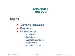
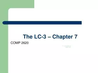
LC3-1 The LC-3 A Review. B. A. PC. ALU. IR. Introduction. In this class we will: Complete the hardware design of the LC-3 Simulate it Run programs on it. Reference Information. You will need the LC-3 Description ECEn 124 / CS 124 Textbook:

E N D
LC3-1The LC-3A Review B A PC ALU IR ECEn 224
Introduction • In this class we will: • Complete the hardware design of the LC-3 • Simulate it • Run programs on it ECEn 224
Reference Information • You will need the LC-3 Description • ECEn 124 / CS 124 Textbook: “Introduction to Computing Systems” (second edition) Yale N. Patt & Sanjay J. Patel McGraw-Hill Higher Education 2004 • Useful Sections (in order of importance): • Appendix A (available on class webpage) • Chapter 5 • Chapter 4 • Reference material available on the class webpage ECEn 224
The Von Neumann Model Memory MAR MDR INPUT * keyboard * mouse * scanner * card reader * disk OUTPUT * monitor * printer * LED * disk Processing Unit TEMP ALU Control Unit PC IR ECEn 224
The Von Neumann Model • Memory is used to store a sequence of instructions • Memory is also used to store data • Memory Address Register (MAR) selects which location in memory will be read or written • Memory Data Register (MDR) contains the data read or to be written Memory MAR MDR ECEn 224
The Von Neumann Model Memory MAR MDR 0000 0001 0010 0011 0100 0101 0110 0111 1000 00011001 11010100 Memory Data Register . . . Memory Address Register ECEn 224
The Von Neumann Model • Arithmetic Logic Unit (ALU) does computations and information processing (ADD, AND, NOT, etc.) • Registers (TEMP) provide a small amount of high-speed temporary storage Processing Unit TEMP ALU ECEn 224
The Von Neumann Model • Control Unit (CU) determines what to do next and controls the rest of the processor • Program Counter (PC) contains the address of the next instruction to be executed • Instruction Register (IR) contains the current instruction being executed Control Unit PC IR ECEn 224
The Von Neumann Model Memory MAR MDR INPUT * keyboard * mouse * scanner * card reader * disk OUTPUT * monitor * printer * LED * disk Processing Unit TEMP ALU Control Unit PC IR Not Enough Time to Study Everything ECEn 224
The Von Neumann Model • Fetch an instruction • Execute it • Repeat (Looks a lot like a State Graph) Execute Fetch ECEn 224
The Instruction Set Architecture (ISA) • ISA for LC-3 • Everything about the computer the software needs to know • Memory organization • Register set • Instruction set • Opcodes • Data types • Addressing modes • Everything the hardware designer needs to know in order to build a computer • Details of how to implement the ISA in hardware are left up to the designer’s imagination ECEn 224
Memory Organization • The LC-3 is a 16-bit machine • All instructions fit into a 16-bit word • Memory is accessed using a 16-bit address word • Its address space is 216 locations (65,536 locations) • Memory is word-addressable • Each location is 16-bits wide (2 bytes each) • Total memory size is 131,072 bytes • The LC-3 is not byte addressable, unlike most machines ECEn 224
Register Set • Memory access is relatively slow • It is outside the processing unit • It requires completion of an instruction to access (LDR) • Registers are inside the processing unit • They can be accessedduringan instruction (ADD) • Nearly all computers have a register set • LC-3 has 8 general purpose registers • Named R0, R1, …, R7 • They are addressed with a 3-bit field in an instruction ECEn 224
Data Types • LC-3 has only one data type • 16-bit two’s complement integer • Other computers have others • 32-bit floating point (float) • 64-bit floating point (double) • 32-bit signed/unsigned (int) • 16-bit signed/unsigned (short) • 8-bit signed/unsigned (char) • Possibly more… These names are system dependent ECEn 224
LC-3 Instructions ADD LD DR DR SR1 SR2 0001 00 0 0010 PCoffset9 ADD LDI DR imm5 1010 PCoffset9 0001 DR SR1 1 AND LDR DR DR SR1 SR2 0101 BaseR 00 0 0110 offset6 DR AND LEA imm5 0101 DR SR1 1 1110 PCoffset9 NOT DR SR SR 1001 111111 ST PCoffset9 0011 STI BR p z 0000 n PCoffset9 SR PCoffset9 1011 JMP STR SR BaseR 1100 0 00 000000 0111 BaseR offset6 JSR TRAP PCoffset11 0100 1 1111 0000 trapvect8 JSRR RTI BaseR 0100 0 00 000000 1000 000000000000 reserved RET 111 1100 0 00 000000 1101 ECEn 224
Anatomy of an Instruction 15 14 13 12 11 10 9 8 7 6 5 4 3 2 1 0 0 0 0 1 1 1 0 0 1 0 0 0 0 1 1 0 Op-Code(tells what the instruction is) Meaning of remaining 12 bits depends on the Op-Code This is a 16-bit instruction format. The instruction always fills one 16-bit word. ECEn 224
A Note About Register Notation • We will often write things like this:R6 = R5 + R3 • What we mean is: • The result of adding the contents of R5 to the contents of R3 is stored into R6 • What does this mean?R6 = R5 + 7 • The result of adding the contents of R5 to the integer 7 is stored into R6 ECEn 224
The Instruction Set • LC-3 has 16 instructions • Three types of instructions • Operate instructions • Operate on data (ADD R6, R2, R5) • Data movement instructions • Memory ↔ registers (LDR R2, R3, #6) • Memory/registers ↔ input/output devices • Control instructions • Change which instruction is executed next (JMP R3) ECEn 224
The Operate Instructions ADD DR SR1 SR2 0001 00 0 ADD imm5 0001 DR SR1 1 AND DR SR1 SR2 0101 00 0 AND imm5 0101 DR SR1 1 NOT DR SR 1001 111111 DR = SR1 + SR2 DR = SR1 + SEXT(imm5) DR = SR1 AND SR2 DR = SR1 AND SEXT(imm5) DR = NOT(SR) ECEn 224
An Operate Instruction ADD R6, R2, R5 15 14 13 12 11 10 9 8 7 6 5 4 3 2 1 0 0 0 0 1 1 1 0 0 1 0 0 0 0 1 0 1 Op-CodeTells what the instruction is SR2 Where the 2nd operand comes from DR Where the result Is stored SR1 Where the 1st operand comes from unused in this instruction R6 R2 R5 ADD R6 = R2 + R5 ECEn 224
The Data Movement Instructions DR = mem [ PC + SEXT(PCoffset9) ] LD DR 0010 PCoffset9 DR = mem [ mem [PC + SEXT(PCoffset9)] ] LDI DR 1010 PCoffset9 DR = mem [ BaseR + SEXT(offset6) ] LDR DR BaseR 0110 offset6 DR = PC + SEXT(PCoffset9) DR LEA 1110 PCoffset9 mem [ PC + SEXT(PCoffset9) ] = SR SR ST 0011 PCoffset9 mem [ mem [PC + SEXT(PCoffset9)] ] = SR STI SR 1011 PCoffset9 mem [ BaseR + SEXT(offset6) ] = SR STR SR 0111 BaseR offset6 ECEn 224
An LDR Instruction LDR R2, R3, 6 15 14 13 12 11 10 9 8 7 6 5 4 3 2 1 0 0 1 1 0 0 1 0 0 1 1 0 0 0 1 1 0 Op-CodeTells what the instruction is DR Where the value fetched from memory will be placed BaseR Where the base address comes from Offset6 Added to contents of BaseR to generate fetch memory address Offset is sign-extended before being added to base R2 R3 6 LDR EffectiveMemoryAddress <= R3 + 6 R2 = MEM[EffectiveMemoryAddress] This requires the computation of an effective memory address. It is base + offset. The contents of R3 are the base address and 6 is the offset. ECEn 224
Control Instructions PC = PC + SEXT(PCoffset9) depending on condition(s) BR p z 0000 n PCoffset9 R7 = PC PC = PC + SEXT(PCoffset11) JSR 0100 1 PCoffset11 R7 = PC PC = BaseR JSRR BaseR 0100 0 00 000000 PC = R7 RET 1100 000 111 000000 Different name,same instruction PC = BaseR JMP BaseR 1100 000 000000 RTI 1000 000000000000 Probably won’t have time to implement these TRAP 1111 0000 trapvect8 ECEn 224
A JSRR Instruction JSRR R3 15 14 13 12 11 10 9 8 7 6 5 4 3 2 1 0 0 1 0 0 0 0 0 0 1 1 0 0 0 0 0 0 unused in this instruction BaseR Where the base address comes from unused in this instruction Op-CodeTells what the instruction is Specifies JSRR as opposed to JSR JSRR R3 R7 <= PC PC <= R3 This is how a subroutine call would be executed. ECEn 224
A JMP Instruction JMP R3 15 14 13 12 11 10 9 8 7 6 5 4 3 2 1 0 1 1 0 0 0 0 0 0 1 1 0 0 0 0 0 0 unused in this instruction BaseR Where the base address comes from Op-CodeTells what the instruction is unused in this instruction JMP R3 PC <= R3 This is how a GOTO statement would be executed. ECEn 224
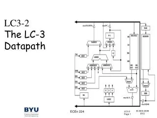
The LC-3 Architecture A More Detailed Look ECEn/CS 224
The LC-3 – Global Bus B A • A bus • Common data highway • multiple on-ramps and off-ramps • Most data transfers between units go across the bus • Example: PC => MAR • Example: MDR => IR • A tri-state driver • Can drive 1’s and 0’s on the bus • Can disconnect from the bus • Control unit turns them on and off PC ALU IR ECEn 224
The LC-3 – Instruction Register (IR) B A • The IR • During a fetch the IR is loaded from the bus • Control unit controls when it should be loaded • Its fields are pulled apart and fed to many places in the circuit • op code • source/destination registers • immediate data • offsets PC ALU IR ECEn 224
The LC-3 – Registers B A • The register file • 8 words of 16-bits each • R0-R7 • Two read address ports • One write address port • Control unit generates control and address signals • To read register file • To write back into the register file PC ALU IR ECEn 224
The LC-3 – ALU B A • The ALU • Does the arithmetic and logical operations on the data • It is always working, results are only stored away at the right time • One input always comes from register file (a) • Second input has two sources • register file (b) • imm5 from instruction (c) • always sign extended (d) • Bit 5 of IR selects 2nd input (e) • Control unit tells ALU which operation to perform (f) PC a b e d f ALU c IR ECEn 224
The Operate Instructions ADD DR SR1 SR2 0001 00 0 ADD imm5 0001 DR SR1 1 AND DR SR1 SR2 0101 00 0 AND imm5 0101 DR SR1 1 NOT DR SR 1001 111111 DR = SR1 + SR2 DR = SR1 + SEXT(imm5) DR = SR1 AND SR2 DR = SR1 AND SEXT(imm5) DR = NOT(SR1) ECEn 224
The LC-3 – Effective Address Block (EAB) B A • The EAB (Effective Address Block) • Calculates effective addresses for the MAR and the PC PC ALU IR ECEn 224
The LC-3 – EAB ADD LD DR DR SR1 SR2 0001 00 0 0010 PCoffset9 ADD LDI DR imm5 1010 PCoffset9 0001 DR SR1 1 AND LDR DR DR SR1 SR2 0101 BaseR 00 0 0110 offset6 DR AND LEA imm5 0101 DR SR1 1 1110 PCoffset9 NOT DR SR SR 1001 111111 ST PCoffset9 0011 STI BR p z 0000 n PCoffset9 SR PCoffset9 1011 JMP STR SR BaseR 1100 0 00 000000 0111 BaseR offset6 JSR TRAP PCoffset11 0100 1 1111 0000 trapvect8 JSRR RTI BaseR 0100 0 00 000000 1000 000000000000 reserved RET 111 1100 0 00 000000 1101 ECEn 224
The LC-3 – EAB ADD LD DR DR SR1 SR2 0001 00 0 0010 PCoffset9 ADD LDI DR imm5 1010 PCoffset9 0001 DR SR1 1 AND LDR DR DR SR1 SR2 0101 BaseR 00 0 0110 offset6 DR AND LEA imm5 0101 DR SR1 1 1110 PCoffset9 NOT DR SR SR 1001 111111 ST PCoffset9 0011 STI BR p z 0000 n PCoffset9 SR PCoffset9 1011 JMP STR SR BaseR 1100 0 00 000000 0111 BaseR offset6 JSR TRAP PCoffset11 0100 1 1111 0000 trapvect8 JSRR RTI BaseR 0100 0 00 000000 1000 000000000000 reserved RET 111 1100 0 00 000000 1101 ECEn 224
The LC-3 – EAB ADD LD DR DR SR1 SR2 0001 00 0 0010 PCoffset9 ADD LDI DR imm5 1010 PCoffset9 0001 DR SR1 1 AND LDR DR DR SR1 SR2 0101 BaseR 00 0 0110 offset6 DR AND LEA imm5 0101 DR SR1 1 1110 PCoffset9 NOT DR SR SR 1001 111111 ST PCoffset9 0011 STI BR p z 0000 n PCoffset9 SR PCoffset9 1011 JMP STR SR BaseR 1100 0 00 000000 0111 BaseR offset6 JSR TRAP PCoffset11 0100 1 1111 0000 trapvect8 JSRR RTI BaseR 0100 0 00 000000 1000 000000000000 reserved RET 111 1100 0 00 000000 1101 ECEn 224
The LC-3 – EAB ADD LD DR DR SR1 SR2 0001 00 0 0010 PCoffset9 ADD LDI DR imm5 1010 PCoffset9 0001 DR SR1 1 AND LDR DR DR SR1 SR2 0101 BaseR 00 0 0110 offset6 DR AND LEA imm5 0101 DR SR1 1 1110 PCoffset9 NOT DR SR SR 1001 111111 ST PCoffset9 0011 STI BR p z 0000 n PCoffset9 SR PCoffset9 1011 JMP STR SR BaseR 1100 0 00 000000 0111 BaseR offset6 JSR TRAP PCoffset11 0100 1 1111 0000 trapvect8 JSRR RTI BaseR 0100 0 00 000000 1000 000000000000 reserved RET 111 1100 0 00 000000 1101 ECEn 224
The LC-3 – EAB B A • The EAB (Effective Address Block) • Calculates effective addresses for the MAR and the PC • It adds two operands that are selected by the control unit (a) • One operand is zero or a sign extended field from the IR (10:0, 8:0, or 5:0) (b) • The other operand is the current value of the PC or the contents of a register from the register file (c) • The sum is passed to both the PCMUX and the MARMUX as an effective address (d) PC d a b c ALU IR ECEn 224
The LC-3 – PC and PCMUX B A • The Program Counter • During the fetch and at the end of some control instructions, the PC is updated to point to the next instruction to be executed • New PC Computation • Can be PC+1 (a) • Can come from global bus (b) • Can come EAB (c) b a PC c ALU IR ECEn 224
The LC-3 – PC and PCMUX B A • Control unit controls loading of PC • Selects which value it should load (a) • Tells when PC should load a new value (b) • Control unit tells PC when to drive onto global bus (c) c b PC a ALU IR ECEn 224
The LC-3 – MARMUX B A • The MARMUX • Selects what address is driven onto global bus for loading into the MAR • MARMUX Sources • Can be IR7:0 zero extended (a) • For TRAP instructions • Can be output of EAB (b) • For load instructions • Control unit selects source (c), controls driving it out onto global bus (d), and when MAR is loaded (e) d e PC c b a ALU IR ECEn 224
The LC-3 – N, Z, P Condition Codes B A • The condition code registers • 1-bit each • Logic block monitors global bus values • It continuously outputs whether bus value is negative, zero, or positive • Control unit controls when N, Z, and P registers are actually loaded • They are loaded on arithmetic and load instructions • Control unit uses them to determine whether or not to branch on BR PC ALU IR ECEn 224
The Memory B A • On a read: • Address comes from MAR • Data is put into MDR and then out onto the bus • On a write: • Address comes from MAR • Data to be written comes from MDR • Control unit tells memory when to load MAR (a), what value to pass through the MDRMUX (b), when to load MDR (c), when to drive the value in the MDR onto global bus (d), and when to write to memory (e). a e PC b c ALU IR d ECEn 224
Data Flow Tracing Data And The Execution of Instructions Through LC-3 ECEn/CS 224
The Von Neumann Model • Fetch an instruction • Execute it • Repeat Execute Fetch ECEn 224
Example Instruction • ADD R5, R2, R6 • Operands must already be in registers 15 14 13 12 11 10 9 8 7 6 5 4 3 2 1 0 0 0 0 1 1 0 1 0 1 0 0 0 0 1 1 0 Op-CodeTells what the instruction is SR2 Where the 2nd operand comes from DR Where the result Is stored SR1 Where the 1st operand comes from Unused in this instruction R5 R2 R6 ADD R5 = R2 + R6 ECEn 224
Instruction Fetch B A a • Copy the PC into the MAR (a) • Load Memory Output into MDR (b) • Load Output of MDR into IR (c) • Increment PC (d) PC d b ALU IR c ECEn 224
Operand Selection B A 101 010 110 0001 00 0 ADD DR SR1 SR2 • Send SR1 and SR2 fields from IR as addresses to the register file (a) • Retrieve values addressed by SR1 and SR2 and send to ALU for execution (b) PC 010 110 b ALU a IR ECEn 224
Execute B A 101 010 110 0001 00 0 ADD DR SR1 SR2 • The ALU does the addition • Control unit tells it whichoperation to do (ADD) PC ADD ALU IR ECEn 224
Store Result B A 101 010 110 0001 00 0 ADD DR SR1 SR2 • Send DR field from IR as address to the register file (a) • Enable ALU output to pass onto the bus (b) • Store ALU output into DR by enabling register file load (c) 101 PC c ALU a IR b ECEn 224
Another Example Instruction • STR R2, R3, 9 • Numbers must already be in registers 15 14 13 12 11 10 9 8 7 6 5 4 3 2 1 0 0 1 1 1 0 1 0 0 1 1 0 0 1 0 0 1 mem [ BaseR + SEXT(offset6) ] = SR Op-CodeSTR SR (R2) BaseR (R3) offset6 (9) is added to contents of BaseR to get the memory location where the contents of SR will be stored EffectiveMemoryAddress <= R3 + 9 mem[EffectiveMemoryAddress] = R2 ECEn 224