Epitaxial Deposition
Epitaxial Deposition. M . H.Nemati Sabanci University. Outline. Introduction Mechanism of epitaxial growth Methods of epitaxial deposition Applications of epitaxial layers. Epitaxial Growth. Deposition of a layer on a substrate which matches the crystalline order of the substrate

Epitaxial Deposition
E N D
Presentation Transcript
Epitaxial Deposition M.H.Nemati Sabanci University
Outline • Introduction • Mechanism of epitaxial growth • Methods of epitaxial deposition • Applications of epitaxial layers
Epitaxial Growth • Deposition of a layer on a substrate which matches the crystalline order of the substrate • Homoepitaxy • Growth of a layer of the same material as the substrate • Si on Si • Heteroepitaxy • Growth of a layer of a different material than the substrate • GaAs on Si Ordered, crystalline growth; NOT epitaxial Epitaxial growth:
Motivation • Epitaxial growth is useful for applications that place stringent demands on a deposited layer: • High purity • Low defect density • Abrupt interfaces • Controlled doping profiles • High repeatability and uniformity • Safe, efficient operation • Can create clean, fresh surface for device fabrication
General Epitaxial Deposition Requirements • Surface preparation • Clean surface needed • Defects of surface duplicated in epitaxial layer • Hydrogen passivation of surface with water/HF • Surface mobility • High temperature required heated substrate • Epitaxial temperature exists, above which deposition is ordered • Species need to be able to move into correct crystallographic location • Relatively slow growth rates result • Ex. ~0.4 to 4 nm/min., SiGe on Si
Thermodynamics • Specific thermodynamics varies by process • Chemical potentials • Driving force • Process involves High temperature process is mass transport controlled, not very sensitive to temperature changes • Close enough to equilibrium that chemical forces that drive growth are minimized to avoid creation of defects and allow for correct ordering • Sufficient energy and time for adsorbed species to reach their lowest energy state, duplicating the crystal lattice structure • Thermodynamic calculations allow the determination of solid composition based on growth temperature and source composition
Kinetics • Growth rate controlled by kinetic considerations • Mass transport of reactants to surface • Reactions in liquid or gas • Reactions at surface • Physical processes on surface • Nature and motion of step growth • Controlling factor in ordering • Specific reactions depend greatly on method employed
Methods of epitaxial deposition • Vapor Phase Epitaxy • Liquid Phase Epitaxy • Molecular Beam Epitaxy
Vapor Phase Epitaxy • Specific form of chemical vapor deposition (CVD) • Reactants introduced as gases • Material to be deposited bound to ligands • Ligands dissociate, allowing desired chemistry to reach surface • Some desorption, but most adsorbed atoms find proper crystallographic position • Example: Deposition of silicon • SiCl4(g) + 2H2(g) ↔ Si(s) + 4HCl(g), • SiCl4 introduced with hydrogen • Forms silicon and HCl gas • SiH4 breaks via thermal decomposition • Reversible and possible to do negative (etching)
Precursors for VPE • Must be sufficiently volatile to allow acceptable growth rates • Heating to desired T must result in pyrolysis • Less hazardous chemicals preferable • Arsine highly toxic; use t-butyl arsine instead • VPE techniques distinguished by precursors used
Reactants are dissolved in a molten solvent at high temperature Substrate dipped into solution while the temperature is held constant Example: SiGe on Si Bismuth used as solvent Temperature held at 800°C High quality layer Fast, inexpensive Not ideal for large area layers or abrupt interfaces Thermodynamic driving force relatively very low Liquid Phase Epitaxy
Molecular Beam Epitaxy • Very promising technique • Beams created by evaporating solid source in UHV • Evaporated beam of particle travel through very high vaccum and then condense to shape the layer • Doping is possible to by adding impurity to source gas by(e.g arsine and phosphors) • Deposition rate is the most important aspect of MBE • Thickness of each layer can be controlled to that of a single atom • development of structures where the electrons can be confined in space, giving quantum wells or even quantum dots • Such layers are now a critical part of many modern semiconductor devices, including semiconductor lasers and light-emitting diodes.
Doping of Epitaxial Layers • Incorporate dopants during deposition(advantages) • Theoretically abrupt dopant distribution • Add impurities to gas during deposition • Arsine, phosphine, and diborane common • Low thermal budget results(disadvantages) • High T treatment results in diffusion of dopant into substrate • Can’t independently control dopant profile and dopant concentration
Applications • Engineered wafers • Clean, flat layer on top of less ideal Si substrate • On top of SOI structures • Ex.: Silicon on sapphire • Higher purity layer on lower quality substrate (SiC) • In CMOS structures • Layers of different doping • Ex. p- layer on top of p+ substrate to avoid latch-up
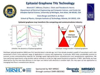
More applications • Bipolar Transistor • Needed to produce buried layer • III-V Devices • Interface quality key • Heterojunction Bipolar Transistor • LED • Laser http://www.search.com/reference/Bipolar_junction_transistor http://www.veeco.com/library/elements/images/hbt.jpg
Summary • Deposition continues crystal structure • Creates clean, abrupt interfaces and high quality surfaces • High temperature, clean surface required • Vapor phase epitaxy a major method of deposition • Epitaxial layers used in highest quality wafers • Very important in III-V semiconductor production
References • P. O. Hansson, J. H. Werner, L. Tapfer, L. P. Tilly, and E. Bauser, Journal of Applied Physics, 68 (5), 2158-2163 (1990). • G. B. Stringfellow, Journal of Crystal Growth, 115, 1-11 (1991). • S. M. Gates, Journal of Physical Chemistry, 96, 10439-10443 (1992). • C. Chatillon and J. Emery, Journal of Crystal Growth, 129, 312-320 (1993). • M. A. Herman, Thin Solid Films, 267, 1-14 (1995). • D. L. Harame et al, IEEE Transactions on Electron Devices, 42 (3), 455-468 (1995). • G. H. Gilmer, H. Huang, and C. Roland, Computational Materials Science, 12, 354-380 (1998). • B. Ferrand, B. Chambaz, and M. Couchaud, Optical Materials, 11, 101-114 (1999). • R. C. Cammarata, K. Sieradzki, and F. Spaepen, Journal of Applied Physics, 87 (3), 1227-1234 (2000). • R. C. Jaeger, Introduction to Microelectronic Fabrication, 141-148 (2002). • R. C. Cammarata and K. Sieradzki, Journal of Applied Mechanics, 69, 415-418 (2002). • A. N. Larsen, Materials Science in Semiconductor Processing, 9, 454-459 (2006).