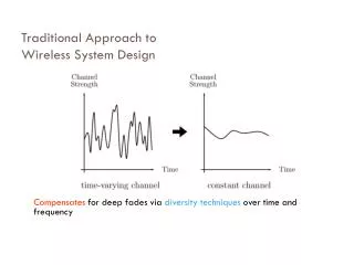
Electronic System Design Wireless 1 Presentation
Electronic System Design Wireless 1 Presentation. Dec 7 th , 2000. Objective Group Designations Timeline System Overview USB Interface Robert TRF6900 Transceiver Robert Antenna Jimmy Testing Imran Packaging Jason Summary & Conclusions Clay Demonstration. Overview.

Electronic System Design Wireless 1 Presentation
E N D
Presentation Transcript
Electronic System DesignWireless 1 Presentation Dec 7th, 2000
Objective Group Designations Timeline System Overview USB Interface Robert TRF6900 Transceiver Robert Antenna Jimmy Testing Imran Packaging Jason Summary & Conclusions Clay Demonstration Overview
PC 1 PC 2 Communication System Communication System Objective • Wireless Communication B/W PC1 & PC2 via USB Port
EVM Group USB Group Antenna Group Testing Group Packaging Group Operation of TRF6900 USB Interface b/w PC & TRF6900 Antenna for Transmission Test Plan & Hardware Issues Package for Final Product Group Designation Wireless Group 1
USB Port EZ-USB Parallel Out Antenna Group USB Group Testing Group Antenna RX_DATA Filtering Circuit Parallel Port TRF6900 Mechanical Antenna Switch EVM Group System Overview Packaging Group
USB Interface & Software Group Group Leader Robert Dickerson Group Members Clay Ayers Asad Khan
Used to diagnose and setup the TRF6900 • Parallel port problems TI Software • Inability to cancel a diagnostic test pattern • Lacked the ability to be used with the USBSIMM
Will program the TRF6900 with the parallel port “Improved” TI Software • Automatically selects USBSIMM when connected • Option to reset settings to default when switching between TX/RX modes • Changed frequency error adjustment to amount of error in the signal • Non-integer testing durations
Chat program with file transfer capabilities InstantSquawker • Uses a basic protocol between itself and the USBSIMM board • Automatically detects and interfaces with the USBSIMM module and programs the TRF6900 on connection
Starting Point Initialize USBSIMM Reset and Disable TRF6900 Do Nothing in Main Loop USB Firmware
Setup packets from the PC USB Firmware • Data packets to send over the RF link • PC request to read the IN buffer • Serial port TX/RX
EVM Group Presentation Group Leader: Imran Bashir Members: Jeff Allen, Asad Khan, Fakhri Sadeh, Wendy Johnston, Jason Benavidez Dec 7th, 2000
TRF6900 Transceiver Transmitter Receiver General Specifications Why TRF6900? Overview
LOCKDET Data Serial Interface Direct Digital Synthesizer (DDS) 2nd Order Loop Filter PLL VCO Tank Circuit Clock Strobe STDBY Mode VCO Crystal Oscillator TX_DATA Antenna Power Amplifier Amplifier Amplifier Filter / Impedance Matching Transmitter
Antenna IF Amplifier (1) RF Amplifier Pre-Select Filter LNA Impedance Matching BPF (1) BPF (1) Carrier RSSI (OOK/ASK) LPF Amplifier/ Post Detection Amplifier IF Amplifier (2) Data Slicer Data Switch FM / FSK Demodulator RX_DATA Tank Circuit Capacitor for VREF External Circuit for LPF Receiver
Parameter Name TRF6900 Frequency (MHz) 850-950 Standard Supported FSK, narrow-band FM Power Output (dBm) 5 Operating Voltage (Volts) 2.2 – 3.6 Standby Current (A) 2 Package 48-pin PQFP SpecificationsTRF6900
Why TRF6900? • Availability • Donation from Texas Instruments • Suitable for the Project’s Objective • Availability of Reference Material & Technical Support
ANTENNA DESIGN GROUP James Furse Aden Wilson
Objectives – Antenna Design • Compact Design • Center Frequency of 915 MHz • Low VSWR • High Gain • Circular Polarization
Objectives – RX/TX Switching • Low Insertion Loss • Fast Switching Speed • TTL Level Input
Antenna Design Scheme • Initial antenna design and evaluation • Optimize characteristics by varying antenna dimensions and configuration • Perform preliminary tests with network analyzer to determine effects of changes • Implement desirable modifications and perform radiation pattern and gain tests
Experimental Modifications • Increased ground plane area • Increased pitch angle • Varied helix diameter • Varied number of helix turns • Implemented shunt feed configuration
Milestones • 10/01/00 Select Antenna Design • 10/08/00 Complete Prototype • 11/15/00 Implement RX/TX Switch • 11/20/00 Successful PC to PC Communication • 12/05/00 Design Complete
NMHA Operation • Normal Mode • Self Resonance • Direction of Maximum Radiation • Elliptical Polarization • Ideal E-Plane Radiation Pattern
Antenna Specifications • Turns 5 • Diameter .3125 • Spacing .48 • Pitch Angle 26 • Helix Length 2.4 • Shunt Feed Configuration
Testing Group Presentation Group Leader: Imran Bashir Members: Jeffery Allen, Asad Khan, Fakhri Sadeh, Farhan Khan Dec 7th, 2000
Overview • Test Setup • Software Issues • Speed • RSSI • Hardware Issue • RX_DATA • Solution • Design 1 • Design 2 • Final Circuit
O’scope OR Logic Analyzer O’scope OR Logic Analyzer Parallel Out EZ-USB USB Port TX_DATA RX_DATA USB Port EZ-USB Parallel Out Duplexer Duplexer TRF6900 EVM TRF6900 EVM DB25 female To DB25 male DB25 female To DB25 male D.C. Power Supply 8 V PC (RX) PC (TX) 8 V Running TRF6900.exe Ver. Beta3 Running TRF6900.exe Ver. Beta 3 Test Setup
Software Issues • Speed • Modified Software for Faster PCs • RSSI • Very Weak Signal from TRF6900 • Turn RSSI “ON” in Software
Voltage Spikes Hardware IssuesNoise Issue • Spikes on RX_DATA During FSK Test
Hardware IssuesNoise Issue • Noise on RX_DATA After FSK Test
Vcc Input A Input B GND Input A Input B Output Hardware IssuesNoise Issue: Solution
Hardware IssuesNoise Issue: Solution • 1st Design TLV3402 Analog Comparator
Hardware IssuesNoise Issue: Solution • Problem: • RSSI Signal is High After FSK Test During FSK Test After FSK Test
Hardware IssuesNoise Issue: Solution • 2nd Design • Cleans Spikes in RX_DATA • High Output After FSK Test

