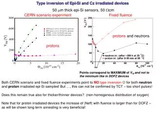
Download
1 / 24
240 likes | 378 Vues
Comparison of P- and N-TYPE structures for both un-irradiated and irradiated MSSD sensors. Simulation of MSSD : C int vs. V bias ( un-irradiated). N type. P type. Simulation is mostly in good agreement with measurements for both P and N - type. Five Trap model.

E N D
Comparison of P- and N-TYPE structures for both un-irradiated and irradiated MSSD sensors
Simulation of MSSD : Cintvs. Vbias (un-irradiated) N type P type • Simulation is mostly in good agreement with measurements for both P and N-type.
Five Trap model • Two shallow acceptors and one • shallow donor in addition to two deep levels • Able to remove accumulation e- • Produce very high E field near n+ • Reproduce experimental observed good • Rint and Cint • With one deep acceptor, it is not possible to create enough E field (similar to measurement) • near n+ strip along with correct current. • We can not use deep acceptors with higher introduction rates as it will change space charge • significantly leading to very high avalanche multiplication & simulated current become very • high compare to measured one. • Moreover, in reality also, shallow levels are created in much more amount compare to deep • trap levels
Simulation of MSSD : Cintvs. Vbias(Irradiated) Red- Experimental result (flux-5e14) Blue - Flux=5e14neq, & QF =8e11cm-2 Green – Flux=1e15neq, & QF=1.2e12cm-2 Red- Experimental result (flux-5e14) Blue - Flux=5e14neq, & QF =8e11cm-2 Green – Flux=1e15neq, & QF=1.2e12cm-2 N type P type • Simulation is mostly in good agreement with measurements for both P and N-type • Cint changes slightly with change in combination of bulk damage (flux) + surface damage (QF)for low bias values.
Simulation of MSSD : Rint vs. Vbias (un-irradiated) N type P type Structure no-1 QF= Vary P type • N-type: • All 12 structures follow the similar good Rint characteristics for all values of QF. • P-Type: • Good isolation for all 12 structures for low values of QF. • Strip-isolation decreases on increasing the QF. QF= 1x1011cm-2 QF= 3x1011cm-2
Simulation of MSSD : Rint vs. Vbias(Irradiated) : P-TYPE • Measurement (Wolfgang) • DC-CAP Simulation (flux = 1x1015 cm-2) P and Y types Different QF • Simulated Rint show trends similar to the Measurements. • Rint decreases on increasing the QF. • Rint is a strong function of the combination of surface damage (QF) and Bulk Damage (flux). Bulk damage compensates for surface damage. • Good isolation even at high flux and high QF. Simulation Different Flux QF = 5x1011cm-2
Simulation of MSSD : Rint vs. Vbias (Irradiated) : N-type • Measurement (Wolfgang) • DC-CAP Simulation (flux = 1x1015 cm-2) Different Structures N-Type: Different QF • Isolation remains good for all values of QF. • Simulation shows decrease in Rint for high values of QF at high Bias values. Experimentally different structures show similar behaviour. • Electric field near the curvature of p+ strip is quite high & increases with QF . This high E field can initiate a localized avalanche & can decrease Rint
Simulation of MSSD : E. Field (Irradiated): P & N-types Efield along the surface (1.3 um below) Efield along the surface (0.1 um below) P-Type P-Type N-Type N-Type Flux = 1x1015cm-2; QF = 1.2x1012cm-2; Bias = 500 V • Peak electric field is more for N-type as compared to P-type sensor for a given bias. • Micro-discharge possibility is more in N-type sensors.
Simulation of MSSD : E. Field (Irradiated): QF variation P-Type N-Type Flux = 1x1015cm-2; QF : Vary ; Bias = 500 V • N-TYPE: • As QF increases = > Peak Efield increases. • Micro-discharge possibility is more in N-type sensors. • P-TYPE: • As QF increases = > Peak Efield decreases.
Simulation of MSSD : E. Field (Irradiated): Temp. variation Efield along the surface (0.1 um below) N-Type Flux = 1x1015cm-2; QF = 8x1011cm-2 ; Bias = 500 V • N:TYPE : Peak E field increases with increase in Temperature.
Effect of P-stop doping concentration : Rint Pstop-5e17cm-3 Pstop – 5e17cm-3 Pstop-5e16cm-3 Bias = 200V Flux=1e15cm-2 QF = 1.5e12cm-2 Cutline is 0.1µm below SiO2 Rint (ohm) Pstop-5e15cm-3 E field (V/cm) P-stop doping conc. Variation; QF=1.2e12 • Strip pitch : 90 micron (width = 20 micron) • Double Pstops (4µm each, separation - 6µm) • Flux = 1e15cm-3 Pstop – 5e15cm-3 • Increase in Pstop-doping conc. Increases Rint but decreases breakdown voltage. • Higher Pstop doping leads to very high E field at lower biases near Pstop curvature which can lead to sensor breakdown or probably microdischargesalso. • Lower Pstop-doping concentration is preferred.
Effect of P-stop doping width : Rint • Strip pitch : 90 micron (width = 20 micron) • Single Pstop (14µm and 28µm ); Pstop doping conc. = 5x1016cm-3 • Flux = 1e15cm-3 • For the values of the Pstop width considered in the simulation, the results of Rint and Efield are almost independent of that.
Effect of QF variation for Pstop = 5e16cm-3 E field (V/cm) • For low values of QF, E field peak is under MO as well as near Pstop also • For higher values of QF, very high E field peak near Pstops, which increases with • increase in QF
Back up-One of the Rint measurement (Robert Eber) Measurement Simulation • Simulation indicate toward QF ~ 1.2e11 cm-2 • Good measurements can be used to predict value of QF using simulations!
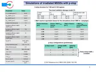
Simulation structures and defects • Three strip structure (dimensions that of no-5 ) having central strip and two neighboring strips • which are shorted together • For Rint simulations, a small 0.2V bias is given to Anode1 electrode and Rint is calculated from • difference in Anode1 and Anode2 currents. • Simulations were carried out for structure having double Pstop isolation structure (The width • of each pstop is 4µm and they are separated by 6µm, pstop doping depth 1.5µm and doping • density 5x1015cm-3 ) and without any isolation structure at all.
Simulation of Rint without any bulk damage • - Three different type of Rint curves were observed. • -For low values of QF, good strip isolation was observed. • For intermediate values of QF, strip isolation is very poor for low biases but improves with higher • reverse biases. Electrons from accumulation layer are progressively removed by higher reverse • bias resulting in better Rint. • But for higher values of QF, Rint remain very low even at higher reverse bias. • Further, it can be observed that pstop doping density 5x1015cm-3 is not sufficient (Fig. 2(a) ) to maintain strip isolation with oxide charge density QF= 5x1011cm-2. • Similarly, it can be inferred from figure 2 (b) that without any isolation structure, strip isolation would not be possible, up to 800V, even for QF = 3x1011cm-2. Figure 2 (a) Figure 2 (b) Without any isolation str With HPK Double Pstops 1x10¹¹ 3x10¹¹
Summary • Bulk damage and surface damage models are used to investigate the • strip isolation, micro - discharge problem and higher leakage current • for strip sensors • p+n- sensors are more prone to micro - discharge problem • Because of very high electric fields in curved regions of strips, Strip • sensors can have more leakage current compare to diodes • Rint measurement curves can also be understood qualitatively by • simulations • Further tuning of simulations is going on
Why two more acceptors with higher introduction rates ? – continue… • Ionized Acceptor trap density inside Si sensor • Ionized Shallow levels (green and blue) are much less compare to deep levels (Red color). • Ionized Acceptors just below SiO2/Si • Interface • In some of the region, Ionized shallow • traps (green and blue) are much more • compare to deep one Cutline is 0.1 um below SiO2 Cutline is perpendicular to n+ strip (Through middle)
Why micro discharge is quenched! • E field inside irradiated sensors is a strong function of space charge charge. • So, when breakdown happen near curved area of p+ strip, a lot of free e/h carriers are produced which will change the nearby space charge significantly, changing the electric field, thus stopping the further breakdown. • Moreover, in irradiated sensors, because of presence of high density of traps, free path length of a charge carrier will be very low, particularly in middle of sensors where E field is very low. These fact would stop the avalanche from turning global and continuous
Measurement of E-field in a irradiated Si strip sensor (n+p-)G. Kramberger et all , 2009, IEEE conference E field profile for a non-irradiated sensors <8000V/cm for reverse bias = 200V • E field profile for a irradiated sensors • Can be as high as 80000V/cm, near the strips for reverse bias = 200V ! • - Formation of high density negative space charge near n+ strips (flux=5e14cm-2) - The negative space charge will act as Pspray and increases with irradiation ! Hence, we never had much problem of strip isolations in hadron irradiation expt!
Electron conc. in the interstrip region decreases as flux increases
Rintvs. Vbias(Irradiated) : Strip pitch and Implant width Flux=1e15cm-2 QF = 1.2e12cm-2 • No significant dependence of Rint on changing the strip pitch and width.