Download
1 / 18
180 likes | 311 Vues
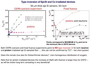
Study of charge collection properties of silicon microstrip detectors with different read out geometries after high doses of proton irradiation. G. Casse, P.P. Allport, S. F. Biagi, T.J.V. Bowcock, A. Greenall, A. Smith, P. Turner. Outline : Introduction

E N D
Study of charge collection properties of silicon microstrip detectors with different read out geometries after high doses of proton irradiation G. Casse, P.P. Allport, S. F. Biagi, T.J.V. Bowcock, A. Greenall, A. Smith, P. Turner • Outline: • Introduction • ISE simulation of non-irradiated and irradiated devices • Non-homogeneous irradiation of large area microstrip detectors • Study of the non-homogenously irradiated detector - CCE(V) and charge sharing - • Signal/noise as a function of the irradiation • Conclusions VERTEX 2002 – Hawaii, 3-7 Nov. 2002
Vfd (a) (b) CCE in silicon diodes before and after irradiation (4 1014 cm-2) The radiation damage introduces charge trapping and changes in VFD, electric field profile, dielectric properties of non-depleted bulk VERTEX 2002 – Hawaii, 3-7 Nov. 2002
Trap type Trap density [cm-3] Energy from mid band gap [V] El. capture cross section [cm-2] Hole capture cross section [cm-2] *Electron 1.50 1015 0.39 1.00 10-14 5.50 10-13 *Electron 2.20 1015 0.13 2.00 10-15 1.20 10-14 Electron 3.60 1014 0.035 1.20 10-15 1.20 10-14 Hole 3.24 1014 -0.045 1.20 10-14 1.20 10-15 *Hole 1.50 1015 -0.20 1.50 10-14 2.00 10-15 We use ISE-TCAD to simulate non-irradiated and irradiated silicon detectors. The radiation effects have been introduced by electron and hole traps in the silicon band-gap. The trap density below corresponds to a fluence of 1x10¹⁵ 1MeV neutron equivalent cm-2. VERTEX 2002 – Hawaii, 3-7 Nov. 2002 * Hallen et al. J. Appl. Phys. 79(1996) 3906
ISE simulation of the electric field profile in a n-bulk silicon diode before and after irradiation (4 1014 p cm-2) p+-implant n+-implant Note the presence of an electric field in the ‘non-depleted’ bulk at low biases and the ‘double-junction’ VERTEX 2002 – Hawaii, 3-7 Nov. 2002
ISE simulation of the majority carrier concentration in a silicon diode before and after irradiation (4 1014 p cm-2) p+-implant n+-implant VERTEX 2002 – Hawaii, 3-7 Nov. 2002
Fluence contours x1014 p/cm2 1 2 3 4 5 6 7 6 5 4 3 2 1 5 Strip #512 4 Strip #384 Strip #640 3 6 Strip #768 Strip #256 2 7 Strip #128 Strip #896 1 8 Inner radius 8mm Outer radius 42mm Non-homogenous irradiation of large area LHCb VELO phi-type prototype detectors VERTEX 2002 – Hawaii, 3-7 Nov. 2002
Irradiated devices : 200 mm n-in-n 200 mm p-in-n 300 mm p-in-n Irradiated together, maximum fluence ~ 7 1014 p cm-2 Maximum fluence ~ 4.6 1014 p cm-2 VERTEX 2002 – Hawaii, 3-7 Nov. 2002
Tools for studying the non-homogeneously irradiated detector: comparison between CCE with infrared (1060 nm) laser and 106Ru ß–source. All measurements with SCT128-VG (LHC speed electronics) CCE(V) for irradiated, 200m thick, detector with laser data (normalised to value at 400V) superimposed VERTEX 2002 – Hawaii, 3-7 Nov. 2002
From fits to the CCE(V), the depletion voltages for the different regions of the detector can be extracted. The Vfd (Neff) profile corresponds to the irradiation profile and allows to study the properties of the detector with a steep gradient of Vfd(Neff). Gradient of Neff can introduces a ‘transverse’ component of the electric field and a distortion in the reconstructed cluster position. Distortions are expected to have opposite sign for opposite sign of the gradient of Neff. VERTEX 2002 – Hawaii, 3-7 Nov. 2002
N-in-n 200 mm detector h= QR/(QR+QL) Strip 517-518 Vfd=29 V Strip 534-535 Vfd=34 V VERTEX 2002 – Hawaii, 3-7 Nov. 2002
h= QR/(QR+QL) N-in-n 200 mm detector Strip 582-583 Vfd=90V Strip 612-613 Vfd=105V Strip 670-671 Vfd=95 V Strp 632-633 Vfd=110V VERTEX 2002 – Hawaii, 3-7 Nov. 2002
P-in-n 300 mm detector h= QR/(QR+QL) Irradiated region with positive gradient of |Neff| as a function of the strip number (Vfd 230 V) Low radiation region Vfd=75V Irradiated region with negative gradient of |Neff| as a function of the strip number (Vfd 230 V) VERTEX 2002 – Hawaii, 3-7 Nov. 2002
No evidence of distortion (spread observed () is approximately 2µm) in the reconstructed cluster position due to the high gradient of Neff in the detector. The experimental results are also supported by ISE simulations VERTEX 2002 – Hawaii, 3-7 Nov. 2002
Signal (106Ru ß–source) degradation as a function of fluence in the non-homogeneous irradiated detector (n-in-n). VERTEX 2002 – Hawaii, 3-7 Nov. 2002
Noise as a function of the applied bias: dose varying from 2. 1014 to 7. 1014 p cm-2 The noise doesn’t change with irradiation and bias (when the total reverse current is kept low, below 1mA) VERTEX 2002 – Hawaii, 3-7 Nov. 2002
The signal/noise measured with this 200 m thick detector with about 7.5 pF input capacitance is about 16 and 12.5 in the non-irradiated and in the most irradiated areas respectively, as measured with the SCT128-VG analogue electronics Signal of fast electrons from 106Ru source (non-irr. area) Cluster significance (irr. area) Cluster significance (non-irr. area) VERTEX 2002 – Hawaii, 3-7 Nov. 2002
For simple one dimensional structures eg large area diodes little difference is expected between the signals seen on the n-side or the p-side. Direct comparisons of n-side and p-side detectors with the same masks fabricated on the same material confirm the superiority of n-side read-out after irradiation. Laser (1060 nm) CCE(V) in the highest irradiated areas for a n-in-n (7. 1014 p cm-2) and p-in-n (6. 1014 p cm-2) 200 m thick microstrip detectors VERTEX 2002 – Hawaii, 3-7 Nov. 2002
Conclusions: • ISE simulations describe well the device properties also after irradiation and successfully predict charge collection properties and are being used for updating designs. • The effect of non-uniform irradiations (with resulting high gradient - 2.6 1012 cm-4 - of Neff across the detector and perpendicular to the strip) has been studied and small limit to the distortion of the reconstructed cluster position have been placed. • The charge collected at a given voltage is reduced both by the trappingand by the changes to the effective doping concentration. • The former is addressed by n-side read-out while the latter can be helped by using an oxygen enhanced substrate. • Combining the techniques of n-side read-out (to reduce the influence of trapping) and enhanced interstitial oxygen should yield tracking detectors good to 1015p/cm2 at least. VERTEX 2002 – Hawaii, 3-7 Nov. 2002