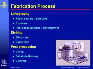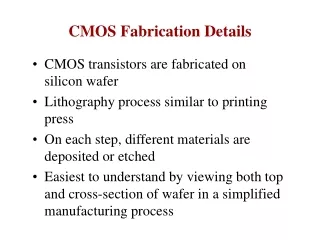
CMOS fabrication process overview
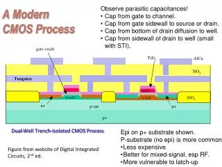
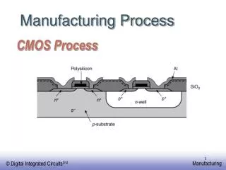
CMOS fabrication process overview. 8-2. P-well on N-substrate. . . . . . . . . Steps : N-type substrateOxidation, and mask (MASK 1) to create P-well (4-5?m deep) P-well doping P-well acts as substrate for nMOS devices. The two areas are electrically isolated using thick field oxide (and often isolation implants [not shown here]).


CMOS fabrication process overview
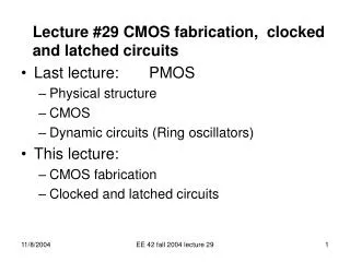
E N D
Presentation Transcript
1. CMOS fabrication process overview 8-1
2. CMOS fabrication process overview 8-2 P-well on N-substrate
3. CMOS fabrication process overview 8-3 Polysilicon Gate Formation
4. CMOS fabrication process overview 8-4 nMOS P+ Source/Drain difusion � self-aligned to Poly gate
5. CMOS fabrication process overview 8-5 pMOS N+ Source/Drain difusion � self-aligned to Poly gate
6. CMOS fabrication process overview 8-6 pMOS N+ Source/Drain difusion, contact holes & metallisation
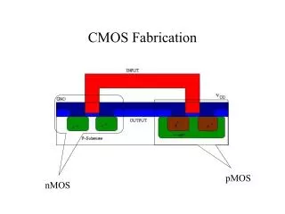
7. CMOS fabrication process overview 8-7 CMOS N-well process
8. CMOS fabrication process overview 8-8
9. CMOS fabrication process overview 8-9
10. CMOS fabrication process overview 8-10