Download
1 / 6
60 likes | 235 Vues
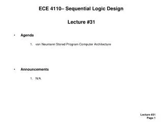
ECE 4110– Sequential Logic Design. Lecture #33 Agenda Timing Announcements Next: Quiz 3. HW #14 assigned. Timing. Physical Timing - physical timing is the circuit delay through various paths and functions within the circuit. A. B. D Q. D Q. Delay. CLK. t setup. CLK A.

E N D
ECE 4110– Sequential Logic Design Lecture #33 • Agenda • Timing • Announcements Next: • Quiz 3. • HW #14 assigned
Timing • Physical Timing- physical timing is the circuit delay through various paths and functions within the circuit A B D Q D Q Delay CLK tsetup CLKA thold AQ A(0) tPLH/PHL tCOMB + tINT BD A(0)
Timing • Physical Timingthold - the time that the data needs to be held constant AFTER the clock edge on a Flop or Register tcomb - the delay through any combinational logic - there are times when thold can be covered by tcomb since the data after a clock edge won't reach the next register until after it propagates tcomb- this works as long as each signal path has at least thold worth of delay in its path. If one signals does NOT, then delay must be added in order to meet tholdtPLH/PHL - the delay it takes for the output of a Flop/Register to appear after a clock edge - this is also called tCQ or "Clock to Q" delay - this can also be called tSEQ to represent the delay through a flop/register tINT - the delay of the interconnect. This is typically modeled as RC delay - this also includes the gate capacitance of any loads (another RC) - estimates typically assume worst case load (Fan-In Spec) and a reasonable trace length
Timing • Physical Timingtsetup - the time that the data must be valid BEFORE a clock edgefMAX - we can do a worst case estimate of delay by assuming tCOMB doesn't cover thold fmax = 1/(thold + tseq + tcomb + tint + tsetup)
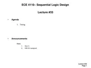
Timing • Pipelined Logic- combinational logic delay can become a significant limitation in large designs- if there was no Fan-In, all logic delay would be a 2-level SOP- but with Fan-In, as the number of inputs grow, levels have to be expanded in order to reduce the number of inputs into each gateex) Fan-In = 2Original (2-level, No Fan-In)Expanded (4 Level, Fan-In Addressed)
Timing • Pipelined Logic- we can break up the combinational logic delay by inserting registers between each level.- this allows the clock frequency to increase because the combinational logic delay is reduced to one-level.- the logic result doesn't occur until after the 3rd clock cycle (this is called "Latency")- if the inputs are continuously coming into the system, they will continually be produced at the output of this "pipelined" circuit after the 3rd clock cycle