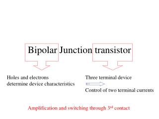
Bipolar Junction Transistor
Bipolar Junction Transistor. Chapter 6 Lecture 7 & 8. The bipolar junction transistor has 3 doped regions. N. COLLECTOR (medium doping). P. BASE (light doping). N. EMITTER (heavy doping). In a properly biased NPN transistor, the emitter electrons


Bipolar Junction Transistor
E N D
Presentation Transcript
Bipolar Junction Transistor Chapter 6 Lecture 7 & 8
The bipolar junction transistor has 3 doped regions. N COLLECTOR (medium doping) P BASE (light doping) N EMITTER (heavy doping)
In a properly biased NPN transistor, the emitter electrons diffuse into the base and then go on to the collector. RC N VCE RB P VCC N VBE VBB
Bipolar Junction Transistors (BJTs) • The bipolar junction transistor is a semiconductor device constructed with three doped regions. • These regions essentially form two ‘back-to-back’ p-n junctions in the same block of semiconductor material (silicon). • The most common use of the BJT is in linear amplifier circuits (linear means that the output is proportional to input). It can also be used as a switch (in, for example, logic circuits).
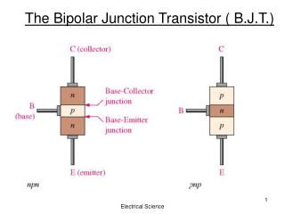
p-type n-type n-type npn-BJT Structure • The ‘npn’ version of the BJT consists of two n regions separated by a p region (as the name suggests). A schematic of an npn transistor is shown.
BJT Structure • The three regions are known as the emitter, base and collector regions. • Electrical connections are made to each of these regions.
E Base (p-type) C Emitter (n-type) Collector (n-type) B npn-BJT Structure
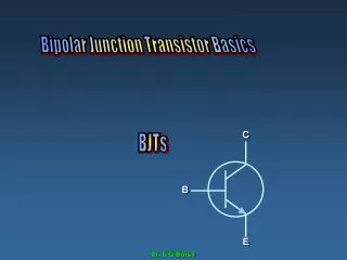
C B E npn BJT Symbol
C B E pnp BJT Symbol • In the symbol for a pnp BJT transistor the direction of the arrow on the emitter is reversed
Still remember about BJT? • The emitter current (iE) is the sum of the collector current (iC) and the base current (iB) • iB << iE and iCOTHER PRAMETERS & • EQUATIONS?
BJT • Basic structure and schematic symbol approximate equivalents transistor symbols pnp type npn type
Refresh.. • Common-emitter current gain, β • Range: 50 < β < 300 • Common-base current gain, α • Range: always slightly less than 1 • The current relationship between these 2 parameters are as follows:
Refresh.. • BJT as amplifying device • B-E junction is forward-biased • B-C junction is reverse-biased
BIASING OF BJT • Remember…! for normal operation • emitter-base junction is always forward-biased AND • collector-base junction is always reverse-biased
Common-Emitter Circuit • with an npn transistor • with a pnp transistor • with a pnp transistor biased with a positive voltage source
IC IC IB IB IE IE IC IC bdc = adc = IB IE Conventional flow Electron flow IE = IC + IB IC @ IE IB << IC
The common emitter connection has two loops: the base loop and the collector loop. RC RB VCE VCC VBE VBB
Subscript notation • When the subscripts are the same, the voltage represents a source (VCC). • When the subscripts are different, the voltage is between two points (VCE). • Single subscripts are used for node voltages with ground serving as the reference (VC).
The base circuit is usually analyzed with the same approximation used for diodes. VBB - VBE RC IB = RB VCE VCC RB VBE VBB
100 mA 80 mA 60 mA 40 mA 20 mA 0 mA A graph of IC versus VCE (Note that each new value of IB presents a new curve.) 14 12 10 IC in mA 8 6 4 2 6 16 2 4 10 12 0 14 18 8 VCE in Volts This set of curves is also called a family of curves.
Regions of operation • Cutoff - - - used in switching applications • Active - - - used for linear amplification • Saturation - - - used in switching applications • Breakdown - - - can destroy the transistor
Transistor circuit approximations • First: treat the base-emitter diode as ideal and use bIB to determine IC. • Second: correct for VBE and use bIB to determine IC. • Third (and higher): correct for bulk resistance and other effects. Usually accomplished by computer simulation.
The second approximation: bdcIB VBE = 0.7 V VCE
VBB - VBE IB = RB 5 V - 0.7 V = 43 mA IB = RC 100 kW 100 kW VCC RB VBE = 0.7 V 5 V VBB
IC = bdc IB IC = 100 x 43 mA = 4.3 mA RC 100 kW bdc = 100 VCC RB IB = 43 mA 5 V VBB
VRC = IC x RC VRC = 4.3 mA x 1 kW = 4.3 V 1 kW RC IC = 4.3 mA 100 kW 12 V VCC RB IB = 43 mA 5 V VBB
IC = 4.3 mA VCE = VCC - VRC VCE = 12 V - 4.3 V = 7.7 V 1 kW RC VCE 100 kW 12 V VCC RB IB = 43 mA 5 V VBB
Typical Breakdown Ratings • VCB = 60 V • VCEO = 40 V • VEB = 6 V • Note: these are reverse breakdown ratings
A graphic view of collector breakdown 14 12 10 IC in mA 8 6 4 2 0 50 VCE in Volts
Typical Maximum Ratings • IC = 200 mA dc • PD = 250 mW (for TA = 60 oC) • PD = 350 mW (for TA = 25 oC) • PD = 1 W (for TC = 60 oC)
Typical “On Characteristics” IC in mA hFE(min) hFE(max) 0.1 40 ___ 1 70 ___ 10 100 300 50 60 ___ 100 30 ___
Troubleshooting • Look for gross voltage errors. • First approximation and mental estimates will usually suffice. • Resistors don’t short but circuit boards can. • Circuit boards can and do open. • Junctions can and do short. • Junctions can and do open.