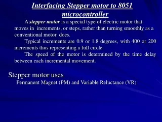
Stepper motor interfacing
Stepper motor interfacing. Full step -clock. Full step –anti clock. ULN 2003. SEVEN DARLINGTONS PER PACKAGE OUTPUT CURRENT 500mA PER DRIVER( 600mA PEAK) OUTPUT VOLTAGE 50V INTEGRATED SUPPRESSION DIODES FOR INDUCTIVE LOADS OUTPUTS CAN BE PARALLELED FORHIGHER CURRENT

Stepper motor interfacing
E N D
Presentation Transcript
Stepper motor interfacing LAKSHMI.B.E.
Full step -clock LAKSHMI.B.E.
Full step –anti clock LAKSHMI.B.E.
ULN 2003 • SEVEN DARLINGTONS PER PACKAGE • OUTPUT CURRENT 500mA PER DRIVER( 600mA PEAK) • OUTPUT VOLTAGE 50V • INTEGRATED SUPPRESSION DIODES FOR INDUCTIVE LOADS • OUTPUTS CAN BE PARALLELED FORHIGHER CURRENT • TTL/CMOS/PMOS/DTL COMPATIBLE INPUTS • INPUTS PINNED OPPOSITE OUTPUTS TO SIMPLIFY LAYOUT LAKSHMI.B.E.
INTERFACING WITH RELAY LAKSHMI.B.E.
ULN 2803 LAKSHMI.B.E.
How to Driving the Relay: • Digitals system and microcontroller pins are couldn’t produce sufficient current to drive the relay. • While relay’s coil’s need 10mA current to be energized. But the microcontroller pin provide a maximum 1-2mA current • For these reason, we place a driver (or) power transistor in between the micro controller and relay LAKSHMI.B.E.
DRIVE CIRCUIT: LAKSHMI.B.E.
INTERFACING WITH OPTOCOUPLER LAKSHMI.B.E.
INTERFACING WITH OPTOCOUPLER LAKSHMI.B.E.
Opto isolator is otherwise called as opto coupler. It isolates two parts of a system. • In an example for driving a motor, the motor can produces back emf. • Back emf is a high voltage spike produced by a sudden change of current. • In ordinary circuits, the unwanted spike voltage is reduced by using decoupling capacitors. • In any systems, that have inductors (coil windings), such as motors, decoupling capacitor or a diode will not reduce the spike voltages. In such cases, opto isolators can be used. LAKSHMI.B.E.
An opto isolator has an LED transmitter and a photo sensor receiver, both are separated from each other by a small gap. • When current flows through the LED, it transmits a light signal to the receiver. • The receiver produces the signal with the same phase but a different current and amplitude. • The opto isolator comes in a small IC Package with four or more pins. There are also packages that contain more than one opto isolator. When placing an opto isolator between two circuits, we must use two separate voltage sources, one for each side LAKSHMI.B.E.
IL 74SINGLE CHANNEL LAKSHMI.B.E.
ILD 74 ILQ74 LAKSHMI.B.E.
7SEGMENT INTERFACING LAKSHMI.B.E.
7 segment displays LAKSHMI.B.E.
CONFIGURATION LAKSHMI.B.E.
COMMON ANODENEGATIVE LOGIC LAKSHMI.B.E.
PIN DIAGRAM +5V SUPPLY LAKSHMI.B.E.
CODES LAKSHMI.B.E.
CONNECTION DIAGRAM LAKSHMI.B.E.
SINGLE DIGIT0 DISPLAY PROGRAM ORG 0H START:MOV P1,#11000000B ACALL DELAY SJMP START DELAY:MOV R1,#255 DELAY1:MOV R2,#255 DELAY2:DJNZ R2,DELAY2 DJNZ R1,DELAY1 RET END LAKSHMI.B.E.
Program Using Rotate Instruction ORG 0H MOV A,#11111110B START: RL A MOV P1,A ACALL DELAY SJMP START DELAY:MOV R1,#255 DELAY1:MOV R2,#255 DELAY2:DJNZ R2,DELAY2 DJNZ R1,DELAY1 RET END LAKSHMI.B.E.
RELATED INSTRUCTIONS AND REGISTER • REGISTER NAME: • DPTR • The Data Pointer (DPTR) is the 8051’s only user-accessible 16-bit (2-byte) register. The Accumulator, "R" registers, and "B" register are all 1-byte values. LAKSHMI.B.E.
INSTRUCTION • DB DEFINE BYTE DIRECTIVES LAKSHMI.B.E.
PROGRAM USING LOOK UP TABLE ORG 0H MOV R0,#10 MOV DPTR,#SEG START :CLR A MOVC A,@A+DPTR MOV P3,A ACALL DELAY INC DPTR DJNZ R2,START DELAY:…………… RET ORG 400H SEG:DB 0c0h,0f9h,0a4h,0b0h,99h, 92h,82h,0f8h, 80h,90h END LAKSHMI.B.E.
INTERFACING 7SEG WITH DECODER LAKSHMI.B.E.
7-SEGMENT WITH DECODER USING LOOKUP TABLE • org 0h • again:mov a,#0h • mov r0,#0h • branch:mov a,r0 • mov dptr,#400h • movca,@a+dptr • mov p2,a • inc r0 • acall delay • cjne r0,#10h, branch • ljmp again LAKSHMI.B.E.
delay:mov r1,#255 • delay1:mov r2,#255 • delay2:djnz r3,delay2 • djnz r2,delay1 • ret • org 400h • decodercode:db 0,1,2,3,4,5,6,7,8,9 • end LAKSHMI.B.E.
MULTIPLEXING LAKSHMI.B.E.
7-SEGMENT MUTLIPLEXING AND SWITCH (Binary Inputs 0-255) ORG 0H MOV P1,#0FFH LOOP:MOV A,P1 MOV B,#100 DIV AB ORL A,#010000000B MOV R0,A MOV A,B MOV B,#10 DIV AB ORL A,#00100000B MOV R1,A MOV A,B LAKSHMI.B.E.
ORL A,#00010000B MOV P3,A ACALL DELAY MOV P3,R1 ACALL DELAY MOV P3,R0 ACALL DELAY SJMP LOOP DELAY:MOV R4,#2 REPEAT:MOV R3,#230 REPEAT1:DJNZ R5, REPEAT1 DJNZ R4, REPEAT RET END LAKSHMI.B.E.
The End LAKSHMI.B.E.