Download
1 / 19
190 likes | 209 Vues
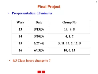
Design either a 16-channel gate driver circuit or a 2-bit 6-channel source driver for TFT-LCD. Detailed project requirements include schematics, SPICE files, timing diagrams, and current/power consumption analysis. Deadline for final report submission is 99/1/14. Contact for assistance: 0935-761741.

E N D
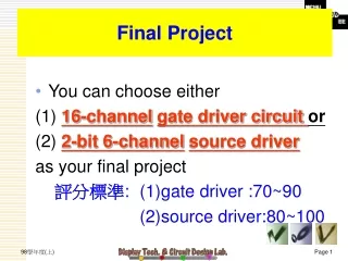
Final Project • You can choose either (1) 16-channelgate driver circuit or (2) 2-bit 6-channelsource driver as your final project 評分標準: (1)gate driver :70~90 (2)source driver:80~100
Flat Panel Display : Principle and Driving Circuit Design • Final Project (1) – 16-channelgate driver circuit • Design a 16-channel gate driver circuit for TFT-LCD • Please use the level shifter shown in next page. • Use H-SPICE with 0.35um model ‘l35uhv12v’ • Use a 5-level RC load (R=2KΩ, C=25pF) • You must finish a final report in power point or Word form before 99/1/14 (17:00) and mail to the teacher.
Level Shifter • Vin=0~Vcc • Vcc=3.0V • Vout=0~AVdd • AVdd=12V
Function block of gate driver • Function block of gate driver circuit 16-bit Shift register Level Shifter Buffer (Inverter) CLK Vout STP Reset Load
Load • 5-level RC load Vout2 Vout1 1-channel Gate Driver Circuit 2K 2K 2K 2K 2K 25pF 25pF 25pF 25pF 25pF
Flat Panel Display : Principle and Driving Circuit Design • The project must include: • Schematics (gate level) of all block • SPICE netlist file • Timing diagram • Vout1, Vout2 & All Control Signals • Rising/falling times • Find current consumption – i(Vcc) & i(Vdda) and Iave(Vcc) & Iave(Vdda) for digital and analog circuits, respectively. • Find total power consumption (instaneous and average). • Discussions ( and what you have learned ) • References
Notice • If you have any problem, please e-mail to me or call 0935-761741.
Flat Panel Display : Principle and Driving Circuit Design • Final Project (2) – 2-bit 6-channelsource driver • 1 persons in a group • Design a 2-bit 6-channel source driver for TFT-LCD • Source driver circuits are based on yourhomework 1~3 • Use Nanosim/Powermill or H-SPICE with 0.35um model ‘l35uhv12v’ • Use a 5-level RC load (R=2KΩ, C=25pF) • You must finish a final report in power point or Word form before 99/1/14 (17:00) and mail to the teacher.
Flat Panel Display : Principle and Driving Circuit Design • The project must include: • Schematics (gate level) of all block (see next page) • SPICE file • Timing diagram • Vin & All Control Signals & Vout : Vin :2-bit for each R、G、B (see page 4~5) • Rising/falling/settling(rise & fall) times • Offset voltages for each level • Find current consumption – i(Vcc) & i(Vdda) and Iave(Vcc) & Iave(Vdda) for digital and analog circuits, respectively. • Find total power consumption (instaneous and average). • Discussions ( and what you have learned ) • References
Block Diagram of Source Driver IC Vdda/Agnd VGAMMA[1-4] Vcc/gnd OUT[1] R[1-2] G[1-2] B[1-2] OUT[2] Analog (LS, DAC, Buffer) OUT[3] 6 bit Digital (SR, Latch1&2) CLK OUT[4] (SHL) POL CLK1 (EQC) OUT[5] OUT[6] DIO2 DIO1
Input Data • 2-bit x R、G、B data input (6-bit) • Red : level 0123… • Green : level1230… • Blue : level2301… • Please run at least 6 clock cycles • Clock frequency = 100 KHz • Please use “dot inversion”
P1 P2 P3 P4 P5 P6 Timing of Input Data 6 CLKs CLK DIO1 DIO2 Data Valid Invalid 6 Outputs for 1~2 Pixel
Digital Circuit Block • Shift Register and Latch SR-1 SR-2 DIO1 DIO2 6 bit Vdata Latch 1 (6x2 bit) CLK Ctrl Latch 2 (6x2 bit) CLK ‘Ctrl’ is generated from ‘CLK1’
Analog Circuit Block Vpos,ref[1-2] Vneg,ref[1-2] POL CLK1 (EQC) ACELL D1[0:1] LVSH SW-P OP OUT1 D2[0:1] LVSH SW-N OP OUT2 D3[0:1] LVSH SW-P OP OUT3 LVSH SW-N OP OUT4 D4[0:1] D5[0:1] LVSH SW-P OP OUT5 LVSH SW-N OP OUT6 D6[0:1]
Level Shifter • Vin=0~3V • Vcc=3V • Vout=0~12V • AVdd=12V
Load Vout1 Vout2 Source Driver Circuit 2K 2K 2K 2K 2K 25pF 25pF 25pF 25pF 25pF
VGamma for DAC • For negative polarity:Vgamma[1]=0.5V,Vgamma[2]=5.0V;negative polarity is from 0.5 to 5V, 4 level, step 1.5V; • For positive polarity:Vgamma[3]=7V,Vgamma[4]=11.5V;positive polarity is from 7 to 11.5V, 4 level, step 1.5V;
Timing Diagram of Output LD is generated from CLK1
Notice • If you have any problem, please e-mail to me or call 0935-761741.