Download
1 / 19
190 likes | 384 Vues
Nanoscale Electronics / Single-Electron Transport in Quantum Dot Arrays. Dene Farrell SUNY Binghamton Research Alliance for Minorities www.csm.ornl.gov Oak Ridge National Laboratory Mentor: Jack Wells, Ph.D. Introduction. Nanotechnology – what is it?

E N D
Nanoscale Electronics / Single-Electron Transport in Quantum Dot Arrays Dene Farrell SUNY Binghamton Research Alliance for Minorities www.csm.ornl.gov Oak Ridge National Laboratory Mentor: Jack Wells, Ph.D.
Introduction • Nanotechnology – what is it? • Science, technology and engineering dealing in nanometer sized dimensions • A nanometer is 1x10⁻⁹ meters • Nanoscale Electronics • Devices of this type are different from their macroscale counterparts • Importance • Research is basic, not applied • Scientists need nanoscale information processors
Project Overview • Goal • Understanding how to observe Coulomb blockade effect in a single-electron device • Procedure • Working mainly on a computational level • Defining transistor properties and analyzing behavior • Results • Greater understanding of Nanoelectronics
Monte-Carlo Single-Electronics Simulator (MOSES) • FORTRAN based simulator program • Utilizing Monte-Carlo method to project transistor performance • Generating Current-Voltage characteristics
Research of single electron transistors involved exposure to new concepts Background research was major component of the internship Key concepts: Electron Tunneling Quantum Dots Coulomb Blockade Coulomb Staircase Background
Electron Tunneling • In classical mechanics, if E < V (the maximum height of the potential barrier), the particle remains in the well forever • If E > V , the particle escapes
Electron Tunneling, Cont. • In Quantum Mechanics, the electron can escape even if its energy E is below the height of the barrier V • Quantum tunneling has no counterpart in classical physics
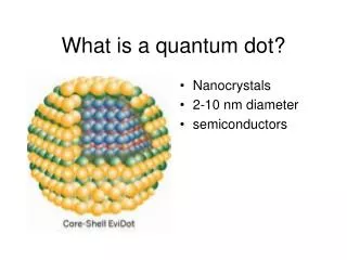
Quantum Dots • “Artificial Atoms” • Quantum Dots Are Clusters of Atoms • Behave like single atom, concerning electron tunneling • Arrays • Single-electron devices often use more than one quantum dot in one, two-dimensional patterns
Requirements: Electron enters or departs island only via “quantum tunneling” Well isolated conductor High resistance tunnel junctions, (Rt >> Rk = h/e2) Charging energy must exceed the energy of thermal fluctuations kbT Ec e2/C >> kbT Very small conductor as C (size) The Coulomb Blockade and the Coulomb Staircase
Atomic force microscope image of gold nanoparticle attached to DNA (a) DNA-nanoparticle assembly, Functionalized gold clusters attached to DNA chain via peptide bonds. (b) Optimized structure of the Au38(SCH3)24 cluster, obtained by quantum molecular dynamics computed on IBM supercomputer at ORNL Directed Bioassembly of Nanoelectronic Arrays
Two-dimensional quantum-dot array showing currents as input channels Iin and output channels Iout Processors for advanced sensors Requires special algorithms Success would result in the first-in-kind application Neuromorphic Signal Discrimination
Acknowledgments This research was performed under the Research Alliance for Minorities Program administered through the Computer Science and Mathematics Division, Oak Ridge National Laboratory. This Program is sponsored by the Mathematical, Information, and Computational Sciences Division; Office of Advanced Scientific Computing Research; U.S. Department of Energy. Oak Ridge National Laboratory is managed by UT-Battelle, LLC, for the U.S. Department of Energy under contract DE-AC05-00OR22725. This work has been authored by a contractor of the U.S. Government under contract DE-AC05-00OR22725. Accordingly, the U.S. Government retains a nonexclusive, royalty-free license to publish or reproduce the published form of this contribution, or allow others to do so, for U.S. Government purposes.
Thank you • A special thanks to Debbie McCoy and Cheryl Hamby for being so caring and helpful and to my mentor, Jack Wells, Ph.D. you were great to work with.
Novel Computational Paradigm Challenge: 1nm-size islands not accessible individually Cannot modulate current in analogy to Field Effect Transistors (FETs) Idea: Control transport with external AC potential Adapt tunneling rate by phase locking to a variable AC potential Supported by experimental evidence Wybourne, et al.,Jpn. J. Appl. Phys., (1997) Clarke, et al.,APL71 (1997) Current Modulation via External AC Potential
Simulation of PAT in QD Arrays • Simulations of PAT in Single-Electron Transport • Modified MOSES to include PAT transition rates • Effective modulation of current by external field • Qualitative agreement with experiments by Wybourne et al