Download
1 / 7
70 likes | 88 Vues
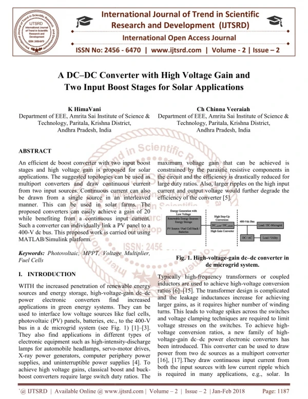
An efficient dc boost converter with two input boost stages and high voltage gain is proposed for solar applications. The suggested topologies can be used as multiport converters and draw continuous current from two input sources. Continuous current can also be drawn from a single source in an interleaved manner. This can be used in solar farms. The proposed converters can easily achieve a gain of 20 while benefiting from a continuous input current. Such a converter can individually link a PV panel to a 400 V dc bus. This proposed work is carried out using MATLAB Simulink platform K Hima Vani | Ch Chinna Veeraiah "A DCDC Converter with High Voltage Gain and Two Input Boost Stages for Solar Applications" Published in International Journal of Trend in Scientific Research and Development (ijtsrd), ISSN: 2456-6470, Volume-2 | Issue-2 , February 2018, URL: https://www.ijtsrd.com/papers/ijtsrd9662.pdf Paper URL: https://www.ijtsrd.com/engineering/electrical-engineering/9662/a-dcu2013dc-converter-with-high-voltage-gain-and-two-input-boost-stages-for-solar-applications/k-hima-vani<br>

E N D
International Research Research and Development (IJTSRD) International Open Access Journal Converter with High Voltage Gain Two Input Boost Stages for Solar Applications International Journal of Trend in Scientific Scientific (IJTSRD) International Open Access Journal ISSN No: 2456 ISSN No: 2456 - 6470 | www.ijtsrd.com | Volume www.ijtsrd.com | Volume - 2 | Issue – 2 A DC–DC Converter Two Input Boost Stages ith High Voltage Gain and or Solar Applications K HimaVani Ch Chinna Veeraiah Ch Chinna Veeraiah Department of EEE, Amrita Sai Institute of Science & Technology, Paritala, Krishna D Andhra Pradesh, India Department of EEE, Amrita Sai Institute of Science & Technology, Paritala, Krishna District, Department of EEE, Amrita Sai Institute of Science & Technology, Paritala, Krishna District, Department of EEE, Amrita Sai Institute of Science & Technology, Paritala, Krishna D Andhra Pradesh Andhra Pradesh, India ABSTRACT An efficient dc boost converter with two input boost stages and high voltage gain is proposed for solar applications. The suggested topologies can be used as multiport converters and draw continuous current from two input sources. Continuous current can also be drawn from a single source in an interleaved manner. This can be used in solar farms. The proposed converters can easily achieve a gain of 20 while benefiting from a continuous input current. Such a converter can individually link a 400-V dc bus. This proposed work is carried out using MATLAB/Simulink platform. Keywords: Photovoltaic, MPPT, Voltage Multiplier, Fuel Cells I.INTRODUCTION An efficient dc boost converter with two input boost stages and high voltage gain is proposed for solar applications. The suggested topologies can be used as multiport converters and draw continuous current maximum voltage gain that can be achieved is ned by the parasitic resistive components in the circuit and the efficiency is drastically reduced for Also, larger ripples on the high input maximum voltage gain that can be achieved is constrained by the parasitic resistive components in the circuit and the efficiency is drastically reduced fo large duty ratios. Also, larger ripples on the high input current and output voltage would further degrade the efficiency of the converter [5]. efficiency of the converter [5]. ous current can also would further degrade the be drawn from a single source in an interleaved manner. This can be used in solar farms. The proposed converters can easily achieve a gain of 20 while benefiting from a continuous input current. Such a converter can individually link a PV panel to a V dc bus. This proposed work is carried out using Photovoltaic, MPPT, Voltage Multiplier, Fig. 1. High-voltage-gain dc dc microgrid system. dc microgrid system. gain dc–dc converter in frequency transformers or coupled inductors are used to achieve high-voltage conversion [15]. The transformer design is complicated and the leakage inductances increase for achieving larger gains, as it requires higher number of winding turns. This leads to voltage spikes across the switches and voltage clamping techniques are required to limit he switches. To achieve high- voltage conversion ratios, a new family of high- dc power electronic converters has converter can be used to draw power from two dc sources as a multiport converter They draw continuous input current from both the input sources with low current ripple which Typically high-frequency transformers or coupled inductors are used to achieve high ratios [6]–[15]. The transformer design is complicated and the leakage inductances increase fo larger gains, as it requires higher number of winding turns. This leads to voltage spikes across the switches and voltage clamping techniques are required to limit voltage stresses on the switches. voltage conversion ratios, a n voltage-gain dc–dc power electronic converters has been introduced. This converter can be used to draw power from two dc sources as a multiport converter [16], [17].They draw continuous input current from both the input sources with low c is required in many applications, e.g., solar is required in many applications, e.g., solar. In WITH the increased penetration of renewable energy sources and energy storage, high-voltage power electronic converters applications in green energy systems. They can be used to interface low voltage sources like fuel cells, photovoltaic (PV) panels, batteries, etc., to the 400 bus in a dc microgrid system (see Fig. 1) [1] They also find applications in different types of electronic equipment such as high-intensity lamps for automobile headlamps, servo X-ray power generators, computer periphery power supplies, and uninterruptible power supplies [4]. To achieve high voltage gains, classical boost and buck boost converters require large switch duty ratios. re large switch duty ratios. The increased penetration of renewable energy voltage-gain dc–dc power applications in green energy systems. They can be used to interface low voltage sources like fuel cells, (PV) panels, batteries, etc., to the 400-V bus in a dc microgrid system (see Fig. 1) [1]–[3]. They also find applications in different types of electronic converters find find increased increased intensity-discharge lamps for automobile headlamps, servo-motor drives, power generators, computer periphery power supplies, and uninterruptible power supplies [4]. To achieve high voltage gains, classical boost and buck- `@ IJTSRD | Available Online @ www.ijtsrd.com @ IJTSRD | Available Online @ www.ijtsrd.com | Volume – 2 | Issue – 2 | Jan-Feb 2018 Feb 2018 Page: 1187
International Journal of Trend in Scientific Research and Development (IJTSRD) ISSN: 2456-6470 conventional approaches, as the output voltage of PV panel is low, several panels are connected in series when connecting the PV array to the 400-V dc bus through conventional step-up converters. This results in reduced system reliability which can be addressed by connecting high-voltage-gain converter to each individual PV panel.Similar interleaved boost input have been proposed earlier using the Cockcroft–Walton (CW) voltage multiplier (VM) [18], [19]. Current fed converters are superior in comparison to the voltage fed counterparts as they have lower input current ripple [19]. The demerit with the CW-based converters is that the output impedance increases rapidly with the number of multiplying stages [20]. Vin1 andVin2. The current in both the inductors rise linearly. The converters with Fig. 3. Switching signals for the input boost stage for the proposed converter Fig. 2. Proposed high-voltage-gain dc–dc converter with four VM stages. I.MODESOFOPERATIONOFCONVERTER The proposed converter is inspired from a Dickson charge pump [20]. Diode-capacitor VM stages are integrated with two boost stages at input. To help the boost stage VM stages are used achieve a higher overall voltage gain. The voltage conversion ratio depends on the number of VM stages and the switch duty ratios of the input boost stages. Fig. 2 shows the proposed converter with four VM stages. For better understanding, the converter operation with four multiplier stages has been explained here. For normal operation of the proposed converter, there should be some overlapping time when both the switches are ON and also one of the switches should be ON at any given time (see Fig. 3). Therefore, the converter has three modes of operation. The proposed converter can operate when the switch duty ratios are small and there is no overlap time between the conduction of the switches. However, this mode of operation is not of interest as it leads to smaller voltage gains. Fig. 4. Mode-I of operation for the proposed converter with four VM stages. Fig. 5. Mode-II of operation for the proposed converter with four VM stages. VM capacitor voltages remain unchanged and the output diode Dout is reverse biased (see Fig. 4); thus, the load is supplied by the output capacitor Cout. A. Mode-I B. Mode-II In this mode, both the switches S1 andS2 are ON. Both the inductors are charged from input sources In this mode, the switch S1 is OFF and S2 is ON (see Fig. 5). All the odd numbered diodes are forward biased and the inductor currentIL1 flows through the `@ IJTSRD | Available Online @ www.ijtsrd.com | Volume – 2 | Issue – 2 | Jan-Feb 2018 Page: 1188
International Journal of Trend in Scientific Research and Development (IJTSRD) ISSN: 2456-6470 VM capacitors charging the odd numbered capacitors (C1,C3,...)and discharging the even numbered capacitors(C2,C4, However, if the number of VM stages is even, then the output diode is forward biased charging the output capacitor and supplying the load. inductorL2, one can write the capacitor voltages (see Fig. 6) in terms of lower boost switching node voltage Where d2 is the switching duty cycle for S2. From (2) and (3), the capacitor voltages for the proposed converter with four VM stages can be derived Fig. 6. Mode-III of operation for the proposed converter with four VM stages. According to, case considered here, since there are four VM stages, the output diode in forward biased. C. Mode-III In this mode, switch S1 is ON and S2 is OFF (see Fig. 6). Now, the even numbered diodes are forward biased and the inductor current IL2 flows through the VM capacitors charging the even numbered capacitors and discharging the odd numbered capacitor. However, if the number of VM stages is even, then the output diode is reverse biased and the load is supplied by the output capacitor. Fig. 7. Proposed converter with N number of VM stages. III. VOLTAGE GAIN OF THE CONVERTER The charge is transferred progressively from input to the output by charging the VM stage capacitors. For the converter with four stages of VM (see Fig. 2), the voltage gain can derived from the volt-sec balance of the boost inductors. For L1, one can write The output voltage is derived from (2), which is given by Similar analysis can be extended to a converter with N number of VM stages (see Fig. 7). Thus, the VM stage capacitor voltages are given by Therefore, from Fig. 5, it can observed that the capacitor voltages can be written in terms of upper boost switching node voltage as When d1is switching duty cycle forS1. Similarly, from the volt-sec balance of the lower leg boost `@ IJTSRD | Available Online @ www.ijtsrd.com | Volume – 2 | Issue – 2 | Jan-Feb 2018 Page: 1189
International Journal of Trend in Scientific Research and Development (IJTSRD) ISSN: 2456-6470 The output voltage equation of the converter with N number of VM stages depends on whether N is odd or even and is given by For N=1, if one combines the topology depicted in Fig. 7 with its alternative (see Fig. 8), then the resulting converter in Fig. 9 is similar to the multiphase converter introduced in [22]. When both topologies with N number of VM stages are combined, the finalised converter is shown in Fig. 10. When N is odd, then from (7) and (10), the voltage gain of the combined topology is given by In this case, the original topology and its alternative each process half of the output power. In other words, the average currents ofDout1andDout2are equal. When N is even, the output voltage of the combined topology would be either (8) or (11) and will be dictated by the topology that provides a higher output voltage. Both legs (see Fig. 10) would compete with each other and only one of the output diodes (Dout1andDout2) would process the entire power while the other will be reverse biased. When Nis even, putting the converters in parallel only makes sense if there is only one source used and d1 =d2. When converter operates in an interleaved manner with single input source, ifd1andd2 are choosen to be an identical, i.e.,d1 =d2 =d, then the output voltage is given by Fig. 8. Alternative to the proposed converter with N number of VM stages. In [21], an interleaved boost power factor corrected converter with voltage-doubler characteristics is introduced. It is worth noting that there is an alternative to the proposed converter (see Fig. 8) where diodeD1 of the first VM stage is connected to the lower boost switching node and capacitorC1 is connected to the upper boost switching node (compare with Fig. 7). The output voltage equation for this alternative topology is given by Fig. 9. Combined topology with single VM stage. Fig. 10. Combined topology with Number of VM stages. `@ IJTSRD | Available Online @ www.ijtsrd.com | Volume – 2 | Issue – 2 | Jan-Feb 2018 Page: 1190
International Journal of Trend in Scientific Research and Development (IJTSRD) ISSN: 2456-6470 output voltage to be For the combined topology with a single input source and identical duty ratiosd1andd2, i.e.,d1 =d2 =d, both the boost stages will always have symmetrical inductor and switch currents irrespective of the number of VM stages. Fig 13. Output Voltage of the Converter. IV.SIMULATIONRESULTS The proposed dc-dc high gain with two input stages for pv systems performance MATLAB/SIMULINK platform. The fig 11 shows the simulated circuit of dc-dc high gain converter and control circuit. The continuous current of two input inductors are shown in fig 12, the output voltage of converter in fig 13. The performance of proposed converter is also analyzed by using it in photovoltaic systems. It is observed that the gain of the converter attains 20. The simulation diagrams of photovoltaic panel and the output current and voltage are also presented. is studied in Fig 14. Simulation diagram of the proposed converter in grid connected PV system. Fig 15. Simulation diagram of DC-DC High Gain Proposed Converter Fig 11. Simulation diagram of DC-DC High Gain Converter Fig 12. Two Input Inductor continuous currents and voltage across Dout. `@ IJTSRD | Available Online @ www.ijtsrd.com | Volume – 2 | Issue – 2 | Jan-Feb 2018 Page: 1191
International Journal of Trend in Scientific Research and Development (IJTSRD) ISSN: 2456-6470 current-fed full bridge converter for fuel cell system,”IEEE Trans. Power Electron., vol. 22, no. 2, pp. 543–550, Mar. 2007. 3)C. Liu and J. S. Lai, “Low frequency current ripple reduction technique with active control in a fuel cell power system with inverter load,”IEEE Trans. Power Electron., vol. 22, no. 4, pp. 1429– 1436, Jul. 2007. 4)E. H. Ismail, M. A. Al-Saffar, A. J. Sabzali, and A. A. Fardoun, “A family of single-switch PWM converters with high step-up conversion ratio,” IEEE Trans. Circuits Syst. I, Reg. Papers, vol. 55, no. 4, pp. 1159–1171, May 2008. Fig 16&17. Modeling of PV panel 5)R. W. Erickson and D. Maksimovic, Fundamentals of Power Electronics, 2nd ed. Norwell, MA, USA: Kluwer, 2001. 6)W. Li and X. He, “A family of interleaved DC– DC converters deduced from a basic cell with winding-cross-coupled inductors (WCCIs) for high step-up or step-down conversions,”IEEE Trans. Power Electron., vol. 23, no. 4, pp. 1791– 1801, Jul. 2008. Fig 18. Grid voltage and grid current. V.CONCLUSION In this paper, a family of novel high-voltage-gain dc– dc converters with two boost stages at the input for photovoltaic applications has been proposed. The proposed converter is based on diode–capacitor VM stages and the voltage gain is increased by increasing the number of VM stages. Power can be drawn from two input sources like a multiport converter in an interleaved manner when connected to single source. One of the advantages of the proposed converter is that since it is a multiport converter with high voltage gain, it has the flexibility to be connected to independent sources while allowing power sharing, MPPT algorithms, etc., independently at each input port. Furthermore, an alternative topology of the proposed converter has been presented and combining them both would result in a new converter topology. The proposed converter can be used for solar applications where each panel can be individually linked to the 400-V dc bus. 7)W. Li and X. He, “An interleaved winding- coupled boost converter with passive lossless clamp circuits,”IEEE Trans. Power Electron., vol. 22, no. 4, pp. 1499–1507, Jul. 2007. 8)W. Li, Y. Zhao, Y. Deng, and X. He, “Interleaved converter with voltage multiplier cell for high step-up and high-efficiency conversion,”IEEE Trans. Power Electron., vol. 25, no. 9, pp. 2397– 2408, Sep. 2010. 9)Y.-P. Hsieh, J.-F. Chen, T.-J. Liang, and L.-S. Yang, “A novel high step-up DC–DC converter for a microgrid system,”IEEE Trans. Power Electron., vol. 26, no. 4, pp. 1127–1136, Apr. 2011. to be implemented 10)R. Xie, W. Li, Y. Zhao, J. Zhao, X. He, and F. Cao, “Performance analysis of isolated ZVT interleaved converter with winding-cross-coupled inductors and switched-capacitors,” in Proc. IEEE Energy Convers. Congr. Expo., Atlanta, GA, USA, 2010, pp. 2025–2029. REFERENCES 1)S. Jain and V. Agarwal, “A single-stage grid connected inverter topology for solar PV systems with maximum power point tracking,”IEEE Trans. Power Electron., vol. 22, no. 5, pp. 1928–1940, Sep. 2007. 11)W. Li, W. Li, X. He, D. Xu, and B. Wu, “General derivation law of nonisolated high-step-up interleaved converters transformer,”IEEE Trans. Ind. Electron., vol. 59, no. 3, pp. 1650–1661, Mar. 2012. with built-in 2)X. Kong and A. M. Khambadkone, “Analysis and implementation of a high efficiency, interleaved `@ IJTSRD | Available Online @ www.ijtsrd.com | Volume – 2 | Issue – 2 | Jan-Feb 2018 Page: 1192
International Journal of Trend in Scientific Research and Development (IJTSRD) ISSN: 2456-6470 12)K.-C. Tseng, C.-C. Huang, and W.-Y. Shih, “A high step-up converter with a voltage multiplier module for a photovoltaic system,”IEEE Trans. Power Electron., vol. 28, no. 6, pp. 3047–3057, Jun. 2013. 14)K.-C. Tseng and C.-C. Huang, “High step-up high-efficiency interleaved converter with voltage multiplier module for renewable energy system,” IEEE Trans. Ind. Electron., vol. 61, no. 3, pp. 1311–1319, Mar. 2014. 13)W. Li, Y. Zhao, J. Wu, and X. He, “Interleaved high step-up converter with winding-cross- coupled inductors and cells,”IEEE Trans. Power Electron., vol. 27, no. 1, pp. 133–143, Jan. 2012. 15)K.-C. Tseng and C.-C. Huang, “A high step-up passive absorption circuit used in non-isolated high step-up converter,” inProc. IEEE Appl. Power Electron. Conf. Expo., Long Beach, CA, USA, 2013, pp. 1966–1971. voltage multiplier `@ IJTSRD | Available Online @ www.ijtsrd.com | Volume – 2 | Issue – 2 | Jan-Feb 2018 Page: 1193