Ch.4 RTL Design
Standard Cell Design. Ch.4 RTL Design. TAIST ICTES Program VLSI Design Methodology Hiroaki Kunieda Tokyo Institute of Technology. 4.1 Basic Components. Logic Design. RTL. RTL Simulation. Logic Synthesis. Scan Netlist. Functional Verification. Scan Path Design.


Ch.4 RTL Design
E N D
Presentation Transcript
Standard Cell Design Ch.4 RTL Design TAIST ICTES Program VLSI Design Methodology Hiroaki Kunieda Tokyo Institute of Technology
Logic Design RTL RTL Simulation Logic Synthesis Scan Netlist Functional Verification Scan Path Design Functional Verification Synthesis Netlist Timing Analysis
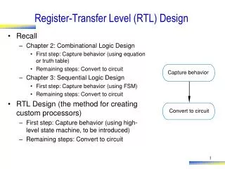
VerilogHDL I This level describes a system by concurrent algorithms (Behavioral). Each algorithm itself is sequential, that means it consists of a set of instructions that are executed one after the other. Functions, Tasks and Always blocks are the main elements. There is no regard to the structural realization of the design. Behavior Level Designs using the Register-Transfer Level specify the characteristics of a circuit by operations and the transfer of data between the registers. An explicit clock is used. RTL design contains exact timing bounds: operations are scheduled to occur at certain times. Modern RTL code definition is "Any code that is synthesizable is called RTL code". RTL Level (Structural Level) Within the logic level the characteristics of a system are described by logical links and their timing properties. All signals are discrete signals. They can only have definite logical values (`0', `1', `X', `Z`). The usable operations are predefined logic primitives (AND, OR, NOT etc gates). Using gate level modeling might not be a good idea for any level of logic design. Gate level code is generated by tools like synthesis tools and this netlist is used for gate level simulation and for backend. Gate Level
VerilogHDL II • reg: memory elements. Substitute in “always” sentence.(<=, =) • wire: signal wire in modules. Substitute in “assign” sentence. • = Blocking substitution, affected by right variable, sequentially. • a = b; • c = a; // c is equivalent to b value • <= Non Blocking, changed by clock timing in parallel. • a <= b; • c <= a; //c and a behaves as shift register. • Signal level:x, o, 1, z • Strength of signal: supply, strong, pull, large, weak, medium, small, highz • parameter: to decide the bit size. • assign #10 x = a & b; //assign after 10 nsec
VerilogHDL III initial begin a = 1’b0; // a=0 at t=0 #10 a = 1’b1; // a=1 at t=10 #20 a = 1’b0; // a=0 at t=20 end Behavior Description with Procedure Block initial: once always: repetitive reg out; wire a, b, sel; always @( a or b or sel ) if(sel = = 1’b1) out = a; else if ( sel = = 1’b0 ) out = b; else out = 1’bx; Note: reg is used in procedure block for left term.
VerilogHDL IV Blocking always @(posedge clock) // q and qr is replaced begin q=d; qr=~d; end Non Blocking //exchange a and b by positive edge of clock always @(posedge clock) begin a<=b; b<=a; end // a=b; b=a; makes both a and b to be old b value.
VerilogHDL V function [ 7 : 0 ] sign_extend; input [ 3 : 0 ] a; if ( a[ 3 ] ) sign_extend = {4’b1111, a }; else sign_extend = {4’b0000, a }; endfunction x <= sign_extend( a ); task sign_extend; input [ 3 : 0 ] a; output [ 7 : 0 ] x; if ( a[ 3 ] ) x= {4’b1111, a }; else x= {4’b0000, a }; endtask sign_extend( a, x ); Tasks are used in all programming languages, generally known as procedures or subroutines. The lines of code are enclosed in task....end task brackets. Data is passed to the task, the processing done, and the result returned. They have to be specifically called, with data ins and outs, rather than just wired in to the general netlist. Included in the main body of code, they can be called many times, reducing code repetition. A Verilog HDL function is the same as a task, with very little differences, like function cannot drive more than one output, can not contain delays. Concatenation 8bit data of sign_extend is made by combining 2 4bits-data
EXOR Gates with Delay module hard_eor(c, a, b); output c; input a, b; wire d, e, f; nand #4 g1(d, a, b); nand #4 g2(e, a, d); nand #4 g3(f, b, d); nand #8 g4(c, e, f); endmodule
Mutiplexer module mux(f, a, b, sel); output f; input a, b, sel; wire not_sel; and g1(f1, a, not_sel), g2(f2, b, sel); or g3(f, f1, f2); not g4(not_sel, sel); endmodule
Decoder module decoder(data_in, data_out); input[1:0] data_in; output[3:0] data_out; always @(data_in) begin case(data_in) 2’b00:data_out<=4’b0001; 2’b01:data_out<=4’b0010; 2’b10:data_out<=4’b0100; 2’b11:data_out<=4’b1000; default: data_out<=4’bxxxx; // the case not described endcase end endmodule
Priority Encoder module encoder(data_in, data_out); input[3:0] data_in; output[1:0] data_out; always @(data_in) begin case(data_in) 4’b0001:data_out<=2’b00; 4’b001x:data_out<=2’b01; 4’b01xx:data_out<=2’b10; 4’b1xxx:data_out<=2’b11; default: data_out<=2’bxx; // the case not described endcase end endmodule
Adder(structure description) module adder(sum, a, b); output sum; input a, b; wire[1:0] a, b; wire[2:0] sum; wire c; half_adder hal(c, sum[0], a[0], b[0]) full_adder fal(sum[2], sum[1], a[1], b[1], c) endmodule
Adder(behavior description) module adder(sum, a, b); parameter size=12, delay=8; input[size-1:0] a, b; output[size-1:0] sum; always @(a or b) #delay s=a+b; endmodule
ALU(Arithmetic and Logic Unit) 6’b101110:out<= in_a & in_b; 6’b110010:out<=~1; 6’b110110:out<= in_a | (~in_b); 6’b111010:out<= in_a| in_b; 6’b111110:out<= in_a; default:out<=x; endcase end endmodule module alu(out, in_a, in_b, cntrl) parameter size=8; input in_a, in_b, ctrl; output out; wire [size-1:0] in_a, in_b, out; wire [5:0] cntrl; always @(cntrl) begin case(cntrl) 6’b000010:out<=~in_a; 6’b000110:out<=~(in_a|in_b); 6’b001010:out<=(~in_a)&in_b; 6’b001110:out<=0; 6’b010010:out<=~(in_a & in_b); 6’b010110:out<=~in_b;
Register module register(data_out, data_in, load, resetn, clk); parameter size=16; input data_in, resetn, clk; output data_out; wire [size-1:0] data_in; reg [size-1:0] data_out; wire resetn, load, clk; always @(posedge clk or negedge resetn); begin if(~resetn) data_out=0; else if(load) data_out=data_in; end endmodule
Counter_Register module counter_register(data_out, data_in, load, inc, resetn, clk); parameter size=16; input data_in, reset, inc, clk; output data_out; wire [size-1:0] data_in; reg [size-1:0] data_out; wire resetn, load, clk; always @(posedge clk or negedge resetn); begin if(~resetn) data_out=0; else if(load) data_out=data_in; else begin if(inc) data_out=data_out+1; end end endmodule
Tristate Buffer (Bus driver) module tristate_buffer(data_out, data_in, enable); parameter size=16; input data_in, enable; output data_out; input[size-1:0] data_in; output[size-1:0] data_out; wire enable; always @(data_in or enable) begin if(enable ==1) data_out=data_in; else if(enable==0) data_out=‘bz; else data_out=‘bx; end endmodule
State Machine parameter s0=2’b00, s1=2’b01, s2=2’b11, s3=2’b10; always @(posedge clock) current_state<=next_state; always @(current_state or input) begin case(current_state) s0: next_state<=(input[0])?s1:s0; s1: next_state<=(input[1])?s2:s0; s2: next_state<=s3; s3: next_state<=s0; default:next_state<=s0; endcase end always @(current_state or input) begin case(current_state) s0: output<=0; s1: output<=0; s2: output<=0; s3: output<=1; default:output<=0; endcase end
Data Path 1 module datapath 1 (InputA, OutputB, loadA, loadB, clk); input InputA, loadA, loadB, clk; Output OutputB wire [7:0] InputA, OutputB; wire load_A, load_B, clk; reg [7:0] OutputA, OutputB; always @(posedge clk) begin if(loadA == 1) OutputA <= InputA; if(loadB == 1) OutputB <= OutputA; end endmodule
module controller(start, Input, loadA, loadB, clk) parameter S0=3’b000, S1=3’b010, S2=3’b100; begin always @(posedge clock) current_state<=next_state; always @(current_state or input) begin case(current_state) S0: next_state<= (Input)?S1:S0; S1: next_state<= S0; S2: next_state<= S1; default:next_state<=s0; endcase endalways @(current_state or input) begin HOLD_REQ=0; ADR_ENn=1; ADR_STB=0; DMA_ACK=0; IOR_OUTn=1; Dbout_STB=0;//default case(current_state) s1: loadA <=1; S2: loadB <=1; endcase endendmodule Controller(State Machine)
PC IR AR Adress_Bus Data_Bus DR INPR OUTR ALU Memory Control words AC F1 Decoder status V Z S C F2 F3 Architecture of Micro Processor
Computer System module CPU(resetn, clk); input resetn, clk; wire [12:0] A_bus; wire [15:0] D_bus; wire [7:0] cntrl1, cntrl2, cntrl3; wire CEn, WEn, OEn; data_path dp1(A_bus, D_bus, cntrl1, cntrl2, cntrl3, resetn, clk); memory sram1(A_bus, CEn, WEn, OEn D_bus); controller cntl1(cntrl1, cntrl2, cntrl3, resetn, clk); endmodule;
Data Path I module data_path(A_bus, D_bus, cntrl1, cntrl2, cntrl3, resetn, clk); input cntrl1, cntrl2, cntrl3, resetn, clk; inout A_bus, D_bus; wire [12:0] A_bus; wire [15:0] D_bus; wire [7:0] cntrl1, cntrl2, cntrl3; wire reestn, clk; reg [15:0] AC_out, IR_out; reg [11:0] PC_out; reg [7:0] INPR_out, OUTR_out; wire [15:0] ALU_out, IR_in; wire [11:0] PC_in; wire [ 7:0] INPR_in, OUTR_in;
Data Path II always // Control Circuits begin AC_in=ALU_out; ld_PC= tbuff_PC= inc_PC= ld_IR= tbuff_IR= op_ALU= ld_AC= tbuff_AC= tbuff_INPR= ld_OUTR= Cen= Oen= WEn-=; end
Data Path III RAM32 ram1(ABUS, CEn, WEn, OEn, DBUS); alu alu1(ALU_out, AC_out, D_bus, c_ALU); register #16 AC1(AC_out, AC_in, ld_AC, resetn, clk); tristate_buffer #16 AC_buffer1(D_bus, AC_out, tbuff_AC); couter_register #12 PC1(PC_out, PC_in, ld_PC, inc_PC, resetn, clk); tristate_buffer #12 PC2(D_bus, PC_out, tbuff_PCDBUS); tristate_buffer #12 PC2(A_bus, PC_out, tbuff_PCABUS); register #16 IR1(IR_out, D_bus, ld_IR, resetn, clk); tristate_buffer #16 IR_buffer1(D_bus, IR_out, tbuff_IRDBUS); tristate_buffer #12 IR_buffer2(A_bus, IR_out[11:0], tbuff_IRABUS); register #8 INPR(INPR_out, INPR_in, ld_INPR, resetn, clk); tristate_buffer #8 INPR_buffer(D_bus, INPR_out, tbuff_INPR); register #8 OUTR(OUTR_out, D_bus, ld_OUTR, resetn, clk); tristate_buffer #8 OUTR_buffer(D_bus, OUTR_out, tbuff_OUTR); endmodule;
Register module register(data_out, data_in, load, resetn, clk); parameter size=16; input data_in, resetn, clk; output data_out; wire [size-1:0] data_in; reg [size-1:0] data_out; wire resetn, load, clk; always @(posedge clk or negedge resetn); begin if(~resetn) data_out=0; else if(load) data_out=data_in; end endmodule
Counter_Register module counter_register(data_out, data_in, load, inc, resetn, clk); parameter size=16; input data_in, reset, inc, clk; output data_out; wire [size-1:0] data_in; reg [size-1:0] data_out; wire resetn, load, clk; always @(posedge clk or negedge resetn); begin if(~resetn) data_out=0; else if(load) data_out=data_in; else begin if(inc) data_out=data_in+1; end end endmodule
Tristate Buffer (Bus driver) module tristate_buffer(data_out, data_in, enable); parameter size=16; input data_in, enable; output data_out; input[size-1:0] data_in; output[size-1:0] data_out; wire enable; always @(data_in or enable) begin if(enable ==1) data_out=data_in; else if(enable==0) data_out=‘bz; else data_out=‘bx; end endmodule
ALU module alu(out, a, b, c_alu) parameter size=8; input a, b, c_alu; output out; wire [size-1:0] a, b, out; wire [2:0] c_alu; always @(c_alu) begin case(c_alu) 3‘b000: out<=a; // trasfer 3'b001: out<= a+1; // increment 3'b010: out<= a +b; // add 3'b011: out<= a+(~b)+1; // subtract 3'b100: out<= b; // load 3'b101: out<= a and b; // and 3'b110: out<= a+(~b)+1; // subtract 3'b111: out<= (~a); // complement default:out<= x; endcase end endmodule
SRAM read cycle CEn=OEn=0
SRAM write cycle WEn Controlled CEn Controlled
Asynchronous SRAM I module RAM32 (A, CEn, WEn, OEn, DQ); input [25:2] Adr; // External memory address inout [31:0] DQ; // External memory data I/O input CEn; // Chip enable input WEn; // Write enable input OEn; // Output enable `define RAMDEPTH 1024 // Memory depth in Kbytes reg [31:0] Ram [0:((`RAMDEPTH * 1024) - 1)]; // Memory register array reg PosedgeWEn; // Rising edge of write enable reg [15:0] Adr_Latch; // Latched address during writes reg [7:0] TRI_DQ; // Tri-state data out
Asynchronous SRAM II always @(posedgeWEn) // Detects the rising edge of WEn begin PosedgeWEn = 1'b1; #5; PosedgeWEn = 1'b0; end //Read Cycle: CEn=OEn=1 always @(CEn or WEn or OEn or Adr or PosedgeWEn) begin if (~CEn & ~OEn & WEn) TRI_DQ = Ram[Adr]; else if (~CEn & ~WEn) begin Adr_Latch = Adr; // Latch address at start of write TRI_DQ = 8'hzz; end
Asynchronous SRAM II else if (PosedgeWEn) begin Ram[Adr_Latch] = DQ; PosedgeWEn = #1 1'b0; // Delay added so that shows up on waveform view end else TRI_DQ = 8'hzz; end assign #2 DQ = TRI_DQ; Endmodule
3bit Counter IR Control Circuit(State Machine Type) Decoder S Z ~FGI ~FGO Combinational Logic CF1[7:0] Control words CF2[7:0] CF3[7:0]
module controller( parameter T0=4’b0000, T1=4’b0001, T2=4’b0010, T3=4’b0011, T4=4’b0100, T5=4’b0101, T6=4’b0110, T7=4’b0111; always @(posedge clock) current_state<=next_state; always @(current_state or input) begin case(current_state) T0: next_state<= (S)?T1:T0; T1: next_state<= T2; T2: next_state<= T3; T3: next_state<= (T)?T4:T0; T4: next_state<= (T)?T5:T0; T5: next_state<= (T)?T6:T0; T6: next_state<= (T)?T7:T0; T7: next_state <= T0; default:next_state<=s0; endcase end Controller(State Machine)
State Machine III (output) end endmodule
DMA Memory Micro Processor I/O Unit DMA Controller DMA stands for Direct Memory Access. I/.O Unit accesses memory Directly while micro processor is idle.
DMA memory to I/O CLOCK DMA_REQ (Input) HOLD_REQ HOLD_ACK(Input) ADR_EN ADR_STB Dbout[7:0] Valid Data Valid data DMA_ACK IOR_OUTn EOP_Inn (Input) (end of operation) S2S3S4S5 S0 S0S0 S0 S0 S1 S1 S3 S4 S5
parameter s0=3’b000, s1=3’b001, s2=3’b010, s3=2’b011, s4=3’b100, s5=3’b101; always @(posedge clock) current_state<=next_state; always @(current_state or input) begin case(current_state) s0: next_state<=(DMA_REQ)?s1:s0; s1: next_state<=(HOLD_ACK)?s2:s1; s2: next_state<=s3; s3: next_state<=s4; s4: next_state<=s5; s5: next_state<=(EOP_Inn)?s0:s3; default:next_state<=s0; endcase end State Machine I