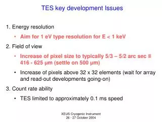
TES key development Issues
This document outlines significant issues related to the development of Transition Edge Sensors (TES) for achieving energy resolution better than 1 eV at energies lower than 1 keV. It discusses expanding the field of view, increasing pixel size to typically 500 μm, enhancing pixel count above 32x32 elements, and counting rate capabilities. Limited speed, current saturation energy levels, and advancements in data analysis algorithms are tackled to improve energy resolution performance. Furthermore, it highlights the implications of these developments for the production of large DROID arrays and the integration of magnetic sensors.

TES key development Issues
E N D
Presentation Transcript
TES key development Issues • Energy resolution • Aim for 1 eV type resolution for E < 1 keV • Field of view • Increase of pixel size to typically 5/3 – 5/2 arc sec ≡ 416 - 625 μm (settle on 500 μm) • Increase of pixels above 32 x 32 elements (wait for array and read-out developments going-on) • Count rate ability • TES limited to approximately 0.1 ms speed XEUS Cryogenic Instrument 26 - 27 October 2004
Energy resolution limit is given by: TES key development Issues with ESAT given by Measured value of EFWHM = 4 eV for C = 0.5pJ/K, α = 70, and T = 100 mK is a factor 3 worse than theory. This is partially due to excess noise and partially due to non-optimum data analysis algorithm. A better data-analysis algorithm should result in 2.5 – 3 eV. Saturation energy equals ≈ 10 keV for r = 0.1 Reduction of the saturation energy to 2.5 keV, C ≈ 1.25 10-13 J/K, would therefore result in an energy resolution improvement by a factor 2.0 Present schemes would than result in ≈ 2 eV energy resolution, while with better data analysis about 1.3 eV is expected. Better understanding and reduction of the excess noise might result in a limit of 0.6 eV FWHM XEUS Cryogenic Instrument 26 - 27 October 2004
Energy resolution limit vs pixel size • We can manufacture standard type pixels with a heat capacity C= 0.125 pJ/K and up to 250 x 250 μm2 • 0.05 pJ/K for TiAu TES • 0.06 pJ/K for Cu/Sn and 0.08 pJ/K for Cu/Bi absorber • Larger pixels will require different designs. Scaling to .5 x .5 mm pixels seems quite well feasible by • Reduction of the fill factor TES/Multiple small TES in parallel • Non-continuous Cu-layer beneath Bi/Sn absorber • Pixels in access of 0.5 x 0.5 mm can most probably not be produced with a saturation at 2.5 keV and its corresponding energy resolution TES key development Issues XEUS Cryogenic Instrument 26 - 27 October 2004
single pixel optimization • single pixel production by micro-electronics techniques • Array production development • Read-out and multiplexing • SQUID development and optimization • How we can use expertise build up for TES development for support of the magnetic sensor line? Magnetic sensor key development Issues XEUS Cryogenic Instrument 26 - 27 October 2004
Prove of good energy resolution for large DROID’s • Arraying of DROID’s • Array read-out electronics STJ sensor key development Issues XEUS Cryogenic Instrument 26 - 27 October 2004
X-ray entrance filters and UV – IR rejection filters • Cryogenics Common key development Issues XEUS Cryogenic Instrument 26 - 27 October 2004