Overview of LEIR Beam Control DSP Board and Daughter Cards
The LEIR Beam Control system is built around a VME board featuring a DSP (ADSP-21160M) using a 32-bit floating-point Super Harvard Architecture clocked at 80 MHz. It supports separate data and instruction buses, a dedicated I/O processor, and has extensive RAM and flash memory for function storage. Multiple daughter cards enhance processing capabilities, enabling advanced digital signal processing, DDS functionalities, and down-conversion, with high-speed data transfer and precise timing interfaces. These components are integral to managing and optimizing beam control operations efficiently.

Overview of LEIR Beam Control DSP Board and Daughter Cards
E N D
Presentation Transcript
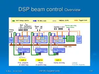
DSP beam control Overview LEIR BC From M.E. Angoletta DSP BC Daughter cards
DSP Board 6 unit VME board with: 1 DSP - ADSP-21160M from Analog Devices – 32 bit floating point – Super Harvard Architecture (SHARC), Clocked at 80 MHz (40 MHz external), 600 MFLOPS - with separate data and instruction busses, dedicated I/O processor with separate bus - 64 bit external data bus clocked at 40 MHz (320 MB/s), 6 byte link Ports at 80 MHz (80 MB/s), 2 serial ports at 40 Mbits/s. 1 MB Flash memory, to restore the DSP software. 4 MB DSP RAM, to store external or calculated functions (like voltage and rf program, steering …) 4 daughter board sites, with two 69 pin connectors for each site 1 Timing interface, based on an AlteraTM FPGA 1 VME interface, based on an AlteraTM FPGA 1 Data interface, based on an AlteraTM FPGA that controls the data flux on Board. 4 MB RAM, for acquisition of internal signals (diagnostics) 16 Trigger inputs (via the RTM) 1 Event link, basically a serial link connected to the rear transition module that allows taking into account 256 events with a hundred ns resolution (not used at CERN). 6 link ports, each portallows up to 8 bit data transfer per DSP internal clock cycle (80 MHz) DSP BC Daughter cards
MDDS Master DDSdaughter card Designed in November 2004 AD9858 1GHz clock DDS ADF4106 PLL + CLV1000A VCO (10MHz => 1 GHz) No SRAM Altera Stratix EP1S10F484C5 2 Tagged clock outputs with IEEE1394 mechanical standard Tagging inside the FPGA with external ELMEC 1.2ns delay (needs control of logical cells placement) DSP BC Daughter cards
IEEE 1394b clock distribution 1.5 ns tag 333 Ms/s equivalent throughput Standard used up to 3.2 Gb/s over 5m cables 9 pin connector LVDS electrical standard 1394b bilingual connector 8 x 5 mm DSP BC Daughter cards
Clock Fan-out VME card Designed in June 2005 1 input with IEEE1394 mechanical standard 1 Optical input / 1 optical output 9 outputs IEEE1394 Delay error between channels below 390 ps DSP BC Daughter cards
DDC Digital Down Converterdaughter card 4 channels 14 bit ADC AD 9245BCP-80 (80 MHz max, 366 mW, pipeline = 7 cycles) 2 MB/10 ns SRAM (1 M x 16 bits) 1 AlteraStratixEP1S20F484C5 1 Tagged clock input with IEEE1394b mechanical standard and de-tagging and divide-by-2 circuit (50% duty cycle and minimum pulse width required by the ADC). DSP BC Daughter cards
DDC Digital Down Converterdaughter card – FPGA content 1 channel / 4 • 4 down mixers with 4 different LO frequencies • Programmable CIC, 0 -> 3 stages, 1 ->15 decimation, 1 -> 255 comb delay, normalization gain • CIC, FIR and LO parameters loaded synchronously with a specific double-tag. Allows on-flight MDDS harmonic change • I/Q frequency discriminator • LO frequency measurement (counter) • 4 different acquisition lines memorizing 4 of 28 different inner signals. Sampling at a chosen sub-harmonic of the main clock. Up to 1 M points per signal at a maximum sampling of 80 MHz. • Channel, CIC, FIR ON/OFF • Reset phase accumulator at each tag DSP BC Daughter cards
SDDS Slave DDSdaughter card 4 channel 14 bit DAC AD 9754BCP-80 (125 MHz max, 185 mW, no pipeline delay) 2 MB/10 ns SRAM (1 M x 16 bits) AlteraStratixEP1S20F484C5 1 Tagged clock input with IEEE1394 mechanical standard and de-tagging and divide-by-2 circuit (50% duty cycle and minimum pulse width required by the ADC). High/Low DAC gain (0 – 18 dB) 17 bit DAC for lowest amplitude signals DSP BC Daughter cards
SDDS Slave DDSdaughter card • 4 up-converters with 4 different LO frequencies • LO parameters loaded synchronously with a specific double-tag. Allows on-flight MDDS harmonic change • LO frequency measurement (counter) • 4 different acquisition lines memorizing 4 of 28 different inner signals. Sampling at a chosen sub-harmonic of the main clock. Up to 1 M points per signal at a maximum sampling of 80 MHz. • Channel ON/OFF • Reset phase accumulator at each tag • Automatic DAC gain setting with respect to required output amplitude • Phase modulation from SRAM DSP BC Daughter cards
DDC with only 2/4 LO’s + only 2nd order FIR And no monitoring of inner signals Stratix 1 FPGA filling-up Compiled with an old version of Quartus; now it is much faster ! DSP BC Daughter cards
Daughter card – FPGA interconnections(Here the DDC) DSP BC Daughter cards
FPGA market(to be completed, very fast survey!) DSP BC Daughter cards
FPGA market(to be completed, very fast survey!) DSP BC Daughter cards
DC to Mother Board data exchange The DSP on the motherboard sends/receives values to/from registers on the Daughter cards. Some of these register values are within a servo loop and the acquisition time is important for the stability of this loop. In the present Leir BC, the data flow within a loop is as follow: The DDC measures I/Q of a variable I/Q is read by the DSP which processes the value taking into account values from other channels, other daughter cards and other DSP boards if required. The DSP process is triggered by a so-called fast clock. A correction value is sent to the MMDS to change the rf clock frequency and possibly parameters of the SDDS DSP BC Daughter cards
DC to Mother Board data exchange DSP BC Daughter cards
Loop delay Rule of thumb: The loop will be sufficiently stable if its delay leads to a phase lag < p/4 at the unity loop gain frequency Loop computation time + Hdw delay < [1/(8.Fmod)] < 21 us for PSB & LEIR (3.Fs=6kHz) < 26 us for PS (3.Fs=4.8 kHz) In LEIR, the in-loop DSP is sampling the data every TS-DSP = 12.5 us (80 kHz). The loop delay within the DSP = import data from DDC (<50ns) + compute error (<7us) + send error to MDDS or SDDS (via another DSP or not < 150 ns) + equivalent 1st order S/H delay (6.25 us) => ≈14us delay within the DSP With a 80 kHz DSP sampling clock, an averaging (CIC) of 1000 80-MHz-samples in the DDC would be adequate. We actually use 256, which means <6.4 us extra delay. This means that we are approaching the reasonable limits required for the LEIR and PSB phase loop. The DSP process time in LEIR is the most time consuming and multiplying by a factor 2 this process speed would almost double the possible bandwidth. DSP BC Daughter cards
Phase jitter within the Loop The error signal within a loop as described in the previous slide is transferred from the rf clock domain (DDC) to another clock domain (DSP) and again into another clock domain (MDDS or SDDS). From DDC to DSP the uncertainty is 1 rf clock period (<25 ns)+ 1 wait state of the DSP (25 ns) The induced phase jitter is (+/- 360o x FMOD) x Δti = +/- 18 mo / kHz of modulation From DDC to MDDS the uncertainty is just 1 MDDS clock period (8 ns)(the 125 MHz on the frequency word acquisition side) The total phase jitter within the loop is thus around +/- 21 mo / kHz of modulation To this value should be added-up the effect of any change in the DSP computation time from one DSP interrupt clock tic to the following and also all the erratic wait states of the DSP acquisitions that occur in between this DDC acquisition to the MDDS frequency change. DSP BC Daughter cards
Communication links With the new motherboard, the Daughter cards will communicate with the DSP via a FPGA. This architecture allows the use of many kinds of communication links, serial or parallel. VME BUS RAM Do we want the “Daughter card” concept, or do we use detached “special function” boards? Do we use one dedicated link for each daughter card or do we share a single link (all cards receiving the interrupt clock)? Other DSP Board Other DSP Board DSP FPGA Other DSP Board Other DSP Board Special Function Board Special Function Board Special Function Board Special Function Board Other DSP Board Special Function Board Special Function Board Other DSP Board Other DSP Board Other DSP Board DSP BC Daughter cards
DC to Mother Board data flow Single 32b transfer: < 25ns+25ns = 50 ns with // DSP bus < 32/800MHz + 20 ns + 8b @ header ? = 60 ns + 10ns? with Gigabit 8b/10b link DSP BC Daughter cards
Conclusion • The FPGA on the daughter cards needs to be upgraded (except MDDS) . It could be the same as the one used on the DSP board (market survey !!) • Finding ADCs and DACs not-requiring 50% duty cycle would allow an increase of the rf sampling clock • Anti-alias filter off-Board or with an easy plug-in / plug-out connector • JTAG connector from VME and Front-Panel • The clock distribution connectors should be more robust, same as for the data serial link (market survey !!) • The data link from DC to FPGA could be serial • Having an ADC (resp. DAC) on a DAC (resp. ADC) board would be convenient and it would allow to use the board for a 1TFBand a TFB (there is a developer available for this job!) DSP BC Daughter cards
Conclusion Possible architecture DSP BC Daughter cards