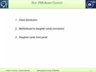
New PSB Beam Control
Summary from previous meeting (27/8/09) ADC comparison DAC comparison Memory comparison FPGA Daughter card interconnection MDDS and its PLL Analogue front-end. New PSB Beam Control . Summary from previous meeting (27/8/09) ADC comparison DAC comparison Memory comparison FPGA

New PSB Beam Control
E N D
Presentation Transcript
Summary from previous meeting (27/8/09) • ADC comparison • DAC comparison • Memory comparison • FPGA • Daughter card interconnection • MDDS and its PLL • Analogue front-end New PSB Beam Control Working group meeting 18/09/2009
Summary from previous meeting (27/8/09) • ADC comparison • DAC comparison • Memory comparison • FPGA • Daughter card interconnection • MDDS and its PLL • Analogue front-end New PSB Beam Control Working group meeting 18/09/2009
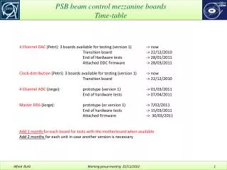
Vita 57 connector between daughter cards and motherboards? • Clock signals from mother board? • Clock connector 1394, eSATA or RJ45? • Vita 57 front panel? • tag and clock on separated twisted pairs sharing the same cable? New PSB Beam ControlSummary from previous meeting Working group meeting 18/09/2009
Summary from previous meeting (27/8/09) • ADC comparison • DAC comparison • Memory comparison • FPGA • Daughter card interconnection • MDDS and its PLL • Analogue front-end New PSB Beam Control Working group meeting 18/09/2009
Expected specifications for the ADC: • Resolution >= 14 bits. The present ADC has 14 bits and a signal to noise and distortion level (SINAD) below 71 dBFS. Although this value seems sufficient for accelerating sychlotrons as LEIR and the PSB, an higher value could be of interest for machine having a higher dynamic range in term of beam current like the AD or for accumulators. • Sampling >= 80 Msps. 80 Msps is the present maximal value. Its is also the value that prevails in many accelerators worldwide. For narrow band cavities, the signal is typically mixed down to 20 MHz and then sampled at 80 MHz to get directly I/Q without further digital mixing. In a context where the direct sampling of the signals has been chosen it is wise to have the highest possible sampling frequency to remove constraints from the anti-alias filter. For example, at the PSB extraction, the h2 beam has a spectrum up to 60 MHz and any signal above the Nyquist limit should be lowered down to less than -96 dBc. It has to be kept in mind that the sampling frequency has a price in term of FPGA, the 80 Msps are marginally achieved now with a Stratix 1 chip. Keep also in mind that in a frequency swept accelerator, 80 MHz max sampling means 40 MHz min sampling. This latter value is the one to be used to dimension the analogue Nyquist filter. • Low power to avoid a heat sink and a possibly required increase of the front panel size • Low latency (pipeline delay < 100 ns at the maximum sampling rate) for more loop stability margins. New PSB Beam Control ADC specifications Working group meeting 18/09/2009
Current ADC AD9245: • 14 bit/80MSPS. • 366mW • 3V single supply • Input BW = 500MHz • Data latency = 7 cycles • Parallel CMOS interface • SINAD -71.2 dBFS at 70MHz • 5 x 5mm with 32 pins • Latest revision 2006 New PSB Beam Control Current ADC: Analog Devices AD9245 Working group meeting 18/09/2009
AD9268: • Dual 16 bit/125MSPS. • 375mW/per channel • 1.8V single supply • Input BW: 625MHz • Data latency = 12 cycles • Parallel CMOS/LVDS interface • SINAD 77.8 dBFS at 70MHz • 9 x 9mm with 64 pins • Latest revision 2009 New PSB Beam Control Alternative ADC: Analog Devices AD9268 Working group meeting 18/09/2009
ADC16V130: • Dual 16 bit/130MSPS. • 650mW = 325mW/channel • 3.3V analog and 1.8V digital supplies • Input BW : 1.4GHz • Data latency = 11 cycles • Parallel CMOS/LVDS interface • SINAD 77.5 dBFS at 70MHz • 9 x 9mm with 64 pins • Latest revision 2009 New PSB Beam Control Alternative ADC: National Semiconductor ADC16V130 Working group meeting 18/09/2009
LTC2208 (LTC2209): • Dual 16 bit/130MSPS (160MSPS) • 1.25W (1.45W) => 625mW/channel • 3.3V single supply • Input BW = 700MHz • Data latency = 7 cycles • Parallel CMOS/LVDS interface • SINAD 77.4 dBFS at 70MHz • 9 x 9mm with 64 pins • Latest revision 2009 New PSB Beam Control Alternative ADC: Linear LTC2209 Working group meeting 18/09/2009
ADS5483: • Dual 16 bit/135MSPS. • 2.2W (= 1100mW/channel !!) • 5V analog and 3.3V digital power supplies • Input BW = 485MHz • Data latency = 5 cycles • Parallel CMOS/LVDS interface • SINAD 77.4 dBFS at 70MHz • 9 x 9mm with 64 pins • Latest revision 2009 New PSB Beam Control Alternative ADC: Texas Instruments ADS5483 Working group meeting 18/09/2009
ADC comparison between the current ADC and alternative choices: New PSB Beam Control ADCs overall comparison Working group meeting 18/09/2009
Summary from previous meeting (27/8/09) • ADC comparison • DAC comparison • Memory comparison • FPGA • Daughter card interconnection • MDDS and its PLL • Analogue front-end New PSB Beam Control Working group meeting 18/09/2009
Block diagram for current DAC AD9754: • 14 bit/125 MSPS • 185mW/1 channel • Settling time = 35ns • Propagation delay 1ns • Single supply +5V • SFDR, 82dBc (at 50 MSPS/1MHz) • Parallel input CMOS/TTL • 9.8 x 4.5mm for 28 pins • Commercially available and cheap • Latest release 1999 • Used in communication, RF and DDS • applications. • A variant: the AD9764 is used in • our section by Daniel and José. It can be powered by a single +3V/45mW at the price of decreased performances (not specified in the datasheet). New PSB Beam Control Current DAC: Analog Devices AD9754 Working group meeting 18/09/2009
Chip layout for current DAC AD9754: New PSB Beam Control Current DAC: Analog Devices AD9754 AD9754 and AD9764 have the same chip layout. The dimensions are 9.8 x 4.5mm for 28 pins. Working group meeting 18/09/2009
Block diagram and chip layout for DAC AD9772A: • 14 bit/160MSPS • 1 channel/single power supply of 3.3V • 272mW (+50% compared to present one) • settling time < 11ns • Propagation delay 17ns • SFDR 82dBc (at 65MSPS/1MHz) • Parallel input CMOS/TTL • 9 x 9mm (double of current) with 48 pins • Integrated interpolation circuit (x2/x4) • Latest release in 2008 New PSB Beam Control Alternative DAC: Analog Devices AD9772A Working group meeting 18/09/2009
Block diagram and chip layout for AD9747: • Dual 16b DAC /250 MSPS • 315mW => 158mW per channel • 3.3V analog and 1.8V digital power supplies • Parallel LVCMOS interface • SFDR 82 dBc (at 250 MSPS/20MHz) • Chip dimensions 10 x 10mm/72 pins • CSP case (pins not going outside the ship borders) • Latest release in 2007 • SAME power per channel • 2 more bits • Twice the speed • Additionally 10-bit auxiliary DACs for external offset nulling and gain scaling for full-scale current for 16-bit DACs 1 and 2 New PSB Beam Control Alternative DAC: Analog Devices AD9747 Working group meeting 18/09/2009
Block diagram for DAC5686: • Dual 16 bit DAC/500MSPS • 445mW/223mW per channel • 3.3V analog and 1.8V digital power • Supplies • Settling time 12ns • Propagation delay 2.5ns • Parallel CMOS interface. • SFDR 89 dBc at 52MSPS/14MHz using x4 interpolation and dual mode • 10 x 10mm with 100 pins • Latest release in 2009 • Integrated 2x-16x interpolation filters New PSB Beam Control Alternative DAC : Texas Instruments DAC5686 Working group meeting 18/09/2009
Chip layout for DAC5686: New PSB Beam Control Alternative DAC : Texas Instruments DAC 5686 Chip dimensions 10 x 10mm with 100 pins. Working group meeting 18/09/2009
DAC5672: New PSB Beam Control Alternative DAC : Texas Instruments DAC5672 • 14 bit dual converter /275 MSPS • 330mW and 165mW/channel • Settling time 20ns • Propagation delay 1.5ns • 3.3V analog and 3.3V digital power • supplies • Parallel CMOS/TTL interface • SFDR 83dBc (at 50MSPS/1MHz) • 10 x 10mm with 48 pins • Latest release in 2009 Working group meeting 18/09/2009
Chip layout for DAC5672: New PSB Beam Control Alternative DAC : Texas Instruments DAC5672 Chip dimensions 10 x 10mm and 48 pins. Working group meeting 18/09/2009
Comparison between current DAC and alternative choices: New PSB Beam Control DAC overall comparison Working group meeting 18/09/2009
Summary from previous meeting (27/8/09) • ADC comparison • DAC comparison • Memory comparison • FPGA • Daughter card interconnection • MDDS and its PLL • Analogue front-end New PSB Beam Control Working group meeting 18/09/2009
1M x 16 bit memory • 10ns access time • 3.3V power supply • 0.990W power dissipation • 54 pins in a ~22x17mm chip • Latest revision 2009 • 10ns access time provides 100MHz sampling frequency. • If we want to have higher speed, we should go under 10ns. New PSB Beam Control Current memory: Cypress CY7C1061BV33 Working group meeting 18/09/2009
1M x 18 bit memory • 3ns access time (250MHz) • 3.3V power supply • 1.5W power dissipation • 100 pins in a 20x14 mm chip • Latest revision 2007 • includes JTAG connectivity New PSB Beam Control Alternative memory: Cypress CY7C1480V33 Working group meeting 18/09/2009
1M x 18 bit memory • 2.6ns access time (250MHz) • 3.3V power supply • 1.0 W power dissipation • 100 pins in a 20x14 mm chip • Latest revision 2006 New PSB Beam Control Alternative memory : Cypress CY7C1372D Working group meeting 18/09/2009
1M x 36 bit memory • 2.6ns access time • 3.3V power supply • 1.7W power dissipation(at 250MHz) • 100 pins in a 20x14mm • chip • Latest revision 2008 New PSB Beam Control Alternative memory: Cypress CY7C1440AV33 Working group meeting 18/09/2009
1M x 36 bit memory • 2.6ns access time • 2.5V power supply • 1.14W power dissipation (at 250MHz) • 100 pins in a 20x14mm • chip • Latest revision 2008 New PSB Beam Control Alternative memory: Cypress CY7C1460AV25 Working group meeting 18/09/2009
2M x 18 bit PSBSRAM • 5ns access time • 3.3V or 2.5V power supply • 1.6W power dissipation • 100 pins in a 20x14mm chip • Latest revision 2008 New PSB Beam Control Alternative memory : Samsung K7A321830C • PSBSRAM = synchronous pipelined burst SRAM memory used as a 2nd level cache of • Pentium and Power PC based system Working group meeting 18/09/2009
1M x 18 bit DDR II memory • 0.45ns access time • 1.8V power supply • 1.52 W power dissipation • 165 pins in a 17x15mm chip • Latest revision 2008 New PSB Beam Control Alternative memory: Samsung K7K1618T2C Working group meeting 18/09/2009
1M x 18 bit QDR memory • 2.5ns access time • 1.8V or 2.5V power supply • 1.04W power dissipation • 165 pins in a 15x13mm chip • Latest revision 2007 New PSB Beam Control Alternative memory : Samsung K7Q161862B Working group meeting 18/09/2009
4M x 18 bit pipelined NtRAM memory • 3.5ns access time • 2.5V power supply • Power dissipation 1.6W • 100 pins in a 20x14mm chip • Latest revision 2008 NtRAM = no turnaround random access memory utilizes all the bandwidth in any combination of operating cycles. Address, data inputs, and all control signals except output enable and linear burst order are synchronized to input clock. New PSB Beam Control Alternative memory: Samsung K7N641845M Working group meeting 18/09/2009
New PSB Beam Control Memory overall comparison Working group meeting 18/09/2009
Summary from previous meeting (27/8/09) • ADC comparison • DAC comparison • Memory comparison • FPGA • Daughter card interconnection • MDDS and its PLL • Analogue front-end New PSB Beam Control Working group meeting 25/07/2009
The current Stratix 1 FPGA is using a 130nm technology. • Its capacity in terms of logic cells and memory doesn’t allow the implementation of all the required circuitry. • Its price increases • The search for new candidates has been achieved within the Altera products line. This choice avoids the redesign of the Quartus files. • 3 different candidates issued from 3 different product families have been compared. Compilation and timing analysis were made implementing the same DDC circuit compiled with Quartus II software. • Were compared to the current Stratix chip, a Cyclone III and a Stratix III chips. Both are engineered with a 65nm technology. • Stratix III device is pin compatible with numerous choices inside the family. LEs can be • upgraded up to 203520. Additionally, cross-family migration is supported between Stratix III and Stratix IV E device families i.e. pin-to-pin compatible. F780 need to be used. • Cyclone III doesn’t offer the same speed grades as the Stratix families do, but they are available at a lower cost. New PSB Beam Control FPGAs Working group meeting 25/07/2009
This table shows the compatible devices within the Stratix and Cyclone families: Note that for stratix 3 there is also the possibility to get a C2 speed grade (not shown here). For the Cyclone 3, C6 is the maximum speed grade. New PSB Beam Control FPGAs Working group meeting 25/07/2009
Summary from previous meeting (27/8/09) • ADC comparison • DAC comparison • Memory comparison • FPGAs • Daughter card interconnection • MDDS and its PLL • Analogue front-end New PSB Beam Control Working group meeting 18/09/2009
In case we would like to adapt to the Vita 57 standard as a daughter card to motherboard interconnection, care should be taken that all the signals being used in the beam control find a location compatible with Vita 57 and its subset defined by the CO group. New PSB Beam Control Daughter card interconnection VITA 57 FMC standard: • Connector stack heights 8.5 and 10 mm • Low Pin Count (LPC) 160 pins and High Pin Count (HPC) 400 pins in a same connector • LPC 68 and HPC 160 user definable pins • Differential and single-ended signaling • 3.3V, 12.0V, adjustable and reference voltage power supply pins • Clock signal pins • JTAG and I2C support pins • MultiGigabit pins (up to 10Gb/s) Working group meeting 18/09/2009
High pin count connector New PSB Beam Control Daughter card interconnection Working group meeting 18/09/2009
Low pin count connector New PSB Beam Control Daughter card interconnection Working group meeting 18/09/2009
New PSB Beam Control Daughter card interconnection Working group meeting 18/09/2009
Summary from previous meeting (27/8/09) ADC comparison DAC comparison Memory comparison FPGAs Daughter card interconnection MDDS and its PLL Analogue front-end New PSB Beam Control Working group meeting 18/09/2009
Current device: AD9858 RefCLK up to 1GHz Fout up to 400MHz 32bit frequency word resolution 14bit phase offset resolution 10bit output DAC Many unused functions as: Automatic frequency ramping Internal PLL Internal analog mixer New PSB Beam Control Digital Direct Synthesizer Stills being a reasonable option. In fully production state. Commercially available. Working group meeting 25/07/2009
Alternative 1: AD9910 RefCLK up to 1GHz Fout up to 400MHz 32bit frequency word resolution 16bit phase offset resolution 14bit output DAC Internal PLL to be used with the reference clock: 7 bit divider, 1GHz internal VCO. New PSB Beam Control Digital Direct Synthesizer Cheaper than the former one. Working group meeting 25/07/2009
Alternative 2: AD9912 RefCLK up to 1GHz Fout up to 400MHz 48bit frequency word resolution 14bit phase offset resolution 14bit output DAC Internal PLL multiplier sub-harmonic output spurious to be studied if used. New PSB Beam Control Digital Direct Synthesizer 4uHz resolution. Working group meeting 25/07/2009
The PLL is used to generate the 1 GHz REFCLK to the DDS from the 10 MHz reference. Some DDS subsystems incorporate an internal PLL which can be used for this task, saving PCB room and costs… The actual PLL being used is the ADF-4106, which is in full production state and is not an expensive part. => We can stay with the actual PLL hardware without any changes, as switching to another model seems not adding any special improvement. New PSB Beam Control PLL Chip Working group meeting 25/07/2009
Summary from previous meeting (27/8/09) • ADC comparison • DAC comparison • Memory comparison • FPGAs • Daughter card interconnection • MDDS and its PLL • Analogue front-end New PSB Beam Control Working group meeting 18/09/2009
The present receiver front-end comprises a Nyquist filter, a broadband differential amplifier and an additional filter to lower the distortions caused by the varying input impedance of the switched capacitor S/H at the input of the ADC. New PSB Beam Control Receiver front-end Each channel uses a different reference voltage source for the A/D converter. Using a common reference voltage source would balance the gains and the dynamic range of all ADC’s. Working group meeting 25/07/2009
ADC input offset compensation: The offset compensation on each analogue input can be automatic. The procedure is as follow: When required by a special event, the analogue input is grounded while the ADC output value is read by the FPGA. This numerical value is the offset. It can be memorized and subtracted to the value obtained during operation: It can also feed a DAC that creates a compensating analogue offset. The analogue compensation has the advantage of keeping the entire dynamic range while the digital compensation doesn’t require any extra hardware. New PSB Beam Control Receiver front-end: offset compensation Working group meeting 25/07/2009
The analogue offset compensation New PSB Beam Control Receiver front-end Working group meeting 25/07/2009
The digital offset compensation New PSB Beam Control Receiver front-end Working group meeting 25/07/2009