Multi-Wire Proportional Chambers for Particle Detection Analysis
210 likes | 293 Vues
Explore the Multi-Wire Proportional Chamber (MWPC) technology, Nobel Prize-winning innovation for particle detection. Learn about operation, parameters, and applications in high-energy physics experiments. Gain insights into drift chambers, resistive wires, timing differences, and tracking methods. Discover applications like ATLAS muon endcap trigger and hadron calorimeters.

Multi-Wire Proportional Chambers for Particle Detection Analysis
E N D
Presentation Transcript
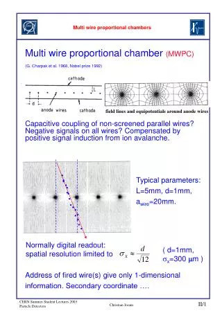
Multi wire proportional chamber(MWPC) (G. Charpak et al. 1968, Nobel prize 1992) Capacitive coupling of non-screened parallel wires? Negative signals on all wires? Compensated by positive signal induction from ion avalanche. Address of fired wire(s) give only 1-dimensional information. Secondary coordinate …. Multi wire proportional chambers field lines and equipotentials around anode wires Typical parameters: L=5mm, d=1mm, awire=20mm. Normally digital readout: spatial resolution limited to ( d=1mm, sx=300 mm ) Christian Joram
Secondary coordinate Charge division. Resistive wires (Carbon,2k/m). Timing difference (DELPHI Outer detector, OPAL vertex detector) 1 wire plane + 2 segmented cathode planes Multi wire proportional chambers Crossed wire planes. Ghost hits. Restricted to low multiplicities. Also stereo planes (crossing under small angle). Analog readout of cathode planes. s 100 mm Christian Joram
Some ‘derivatives’ Derivatives of proportional chambers • Thin gap chambers (TGC) Gas: CO2/n-pentane ( 50/50) Operation in saturated mode. Signal amplitude limited by by the resistivity of the graphite layer ( 40kW/). Fast (2 ns risetime), large signals (gain 106), robust Application: OPAL pole tip hadron calorimeter. G. Mikenberg, NIM A 265 (1988) 223 ATLAS muon endcap trigger, Y.Arai et al. NIM A 367 (1995) 398 Christian Joram
Resistive plate chambers (RPC) Derivatives of proportional chambers No wires ! Gas: C2F4H2, (C2F5H) + few % isobutane (ATLAS, A. Di Ciaccio, NIM A 384 (1996) 222) Time dispersion 1..2 ns suited as trigger chamber Rate capability 1 kHz / cm2 Double and multigap geometries improve timing and efficiency Problem: Operation close to streamer mode. Christian Joram
Drift chambers Drift chambers (First studies: T. Bressani, G. Charpak, D. Rahm, C. Zupancic, 1969 First operation drift chamber: A.H. Walenta, J. Heintze, B. Schürlein, NIM 92 (1971) 373) x Measure arrival time of electrons at sense wire relative to a time t0. What happens during the drift towards the anode wire ? Diffusion ? Drift velocity ? Christian Joram
Drift and diffusion in gases No external fields: Electrons and ions will lose their energy due to collisions with the gas atoms thermalization Undergoing multiple collisions, an originally localized ensemble of charges will diffuse Drift and diffusion in gases D: diffusion coefficient External electric field: “stop and go” traffic due to scattering from gas atoms drift Christian Joram
Drift and diffusion in gases in the equilibrium ... fractional energy loss / collision v: instantaneous velocity s = s(e) ! l = l(e) ! e [eV] (B. Schmidt, thesis, unpublished, 1986) e [eV] Typical electron drift velocity:5 cm/ms Ion drift velocities: ca. 1000 times smaller Christian Joram
In the presence of electric and magnetic fields, drift and diffusion are driven by effects Drift and diffusion in gases Look at 2 special cases: Special case: aL: Lorentz angle cyclotron frequency Transverse diffusion s (mm) for a drift of 15 cm in different Ar/CH4 mixtures Special case: (A. Clark et al., PEP-4 proposal, 1976) The longitudinal diffusion (along B-field) is unchanged. In the transverse projection the electrons are forced on circle segments with the radius vT/w. The transverse diffusion coefficient appears reduced Very useful… see later ! Christian Joram
Drift chambers Some planar drift chamber designs Optimize geometry constant E-field Choose drift gases with little dependence vD(E) linear space - time relation r(t) (U. Becker, in: Instrumentation in High Energy Physics, World Scientific) The spatial resolution is not limited by the cell size less wires, less electronics, less support structure than in MWPC. Christian Joram
Drift chambers (N. Filatova et al., NIM 143 (1977) 17) Resolution determined by • diffusion, • path fluctuations, • electronics • primary ionization statistics Various geometries of cylindrical drift chambers Christian Joram
Time Projection Chamber full 3-D track reconstruction x-y from wires and segmented cathode of MWPC z from drift time in addition dE/dx information Drift Chambers PEP-4 TPC Diffusion significantly reduced by B-field. Requires precise knowledge of vD LASER calibration + p,T corrections Drift over long distances very good gas quality required Space charge problem from positive ions, drifting back to midwall gating ALEPH TPC (ALEPH coll., NIM A 294 (1990) 121, W. Atwood et. Al, NIM A 306 (1991) 446) Gate open Gate closed Ø 3.6M, L=4.4 m sRf = 173 mm sz = 740 mm (isolated leptons) DVg = 150 V Christian Joram
Faster and more precision ? smaller structures Microstrip gas chambers ions C A Micro gaseous detectors (A. Oed, NIM A 263 (1988) 352) geometry and typical dimensions (former CMS standard) Gold strips + Cr underlayer Glass DESAG AF45 + S8900 semiconducting glass coating, r=1016 / Field geometry Fast ion evacuation high rate capability 106 /(mm2s) Gas: Ar-DME, Ne-DME (1:2), Lorentz angle 14º at 4T. Gain104 Passivation: non-conductive protection of cathode edges Resolution: 30..40 mm Aging: Seems to be under control. 10 years LHC operation 100 mC/cm CMS Christian Joram
Micro gaseous detectors • GEM: The Gas Electron Multiplier (R. Bouclier et al., NIM A 396 (1997) 50) Micro photo of a GEM foil Christian Joram
Micro gaseous detectors Single GEM + readout pads Double GEM + readout pads Same gain at lower voltage Less discharges Christian Joram
Silicon detectors Solid state detectors have a long tradition for energy measurements (Si, Ge, Ge(Li)). Here we are interested in their use as precision trackers ! Silicon detectors Si sensor ATLAS SCT Some characteristic numbers for silicon • Band gap: Eg =1.12 V. • E(e--hole pair) = 3.6 eV, ( 30 eV for gas detectors). • High specific density (2.33 g/cm3) DE/track length for M.I.P.’s.: 390 eV/mm 108 e-h/ mm (average) • High mobility: me=1450 cm2/Vs, mh = 450 cm2/Vs • Detector production by microelectronic techniques small dimensions fast charge collection (<10 ns). • Rigidity of silicon allows thin self supporting structures. Typical thickness 300 mm 3.2 104 e-h (average) • But: No charge multiplication mechanism! Christian Joram
How to obtain a signal ? Silicon detectors In a pure intrinsic (undoped) material the electron density n and hole density p are equal. n = p = ni For Silicon: ni 1.451010 cm-3 In this volume we have 4.5 108free charge carriers, butonly 3.2 104e-h pairs produced by a M.I.P. Reduce number of free charge carriers, i.e. deplete the detector Most detectors make use of reverse biased p-n junctions Christian Joram
Doping Silicon detectors p-type: Add elements from IIIrd group, acceptors, e.g. B. Holes are the majority carriers. n-type: Add elements from Vth group, donors, e.g. As. Electrons are the majority carriers. detector grade electronics grade doping concentration 1012 cm-3 (n) - 1015 cm-3 (p+) 1017(18) cm-3 resistivity 5 k·cm 1 ·cm pn junction There must be a single Fermi level ! Deformation of band structure potential difference. Christian Joram
Silicon detectors diffusion of e- into p-zone, h+ into n-zone potential difference stopping diffusion thin depletion zone no free charge carriers in depletion zone (A. Peisert, Instrumentation In High Energy Physics, World Scientific) • Application of a reverse bias voltage (about 100V) the thin depletion zone gets extended over the full junction fully depleted detector. • Energy deposition in the depleted zone, due to traversing charged particles or photons (X-rays), creates free e--hole pairs. • Under the influence of the E-field, the electrons drift towards the n-side, the holes towards the p-side detectable current. Christian Joram
Spatial information by segmenting the p doped layer single sided microstrip detector. Silicon detectors Schematically ! ca. 50-150 mm readout capacitances SiO2 passivation 300mm (A. Peisert, Instrumentation In High Energy Physics, World Scientific) defines end of depletion zone + good ohmic contact ALICE: Single sided micro strip prototype Christian Joram
Silicon pixel detectors Segment silicon to diode matrix also readout electronic with same geometry connection by bump bonding techniques Requires sophisticated readout architecture First experiment WA94 (1991), WA97 OMEGA 3 / LHC1 chip (2048 pixels, 50x500 mm2) (CERN ECP/96-03) Pixel detectors will be used also in LHC experiments (ATLAS, ALICE, CMS) Silicon detectors Flip-chip technique RD 19, E. Heijne et al., NIM A 384 (1994) 399 Christian Joram
The DELPHI micro vertex detector (since 1996) Silicon Detectors 50 mmRf 44-176 mm z 50 mmRf 50-150 mm z 200 mmSS 1033 mm, 10º q 170º 50 mmRf 50-100 mm z 330 x 330 mm2 readout channels ca. 174 k strips, 1.2 M pixels total readout time: 1.6 ms Total dissipated power 400 W water cooling system Hit resolution in barrel part 10 mm Impact parameter resolution (rf) Christian Joram