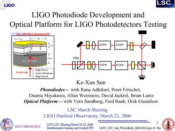
Advanced LIGO Photodiode Development ______
Advanced LIGO Photodiode Development ______. David Jackrel, PhD Candidate Stanford University Dept. of Materials Science and Engineering James S. Harris Hannover, Germany August 20 th , 2003 LIGO-G030495-00-Z. Outline. Motivation & Introduction AdLIGO PD Specifications

Advanced LIGO Photodiode Development ______
E N D
Presentation Transcript
Advanced LIGO Photodiode Development______ David Jackrel, PhD Candidate Stanford University Dept. of Materials Science and Engineering James S. Harris Hannover, Germany August 20th, 2003 LIGO-G030495-00-Z
Outline • Motivation & Introduction • AdLIGO PD Specifications • Device Materials and Design InGaAs vs. GaInNAs • Device Results • Thinned Device QE • InGaAs & GaInNAs I-V • 2m Thick GaInNAs Absorption • Predictions
Auxiliary Length Sensing Power Stabilization Advanced LIGO Schematic
e.g. 1W/0.70=1.43W Resonating Tank Circuit Thinned Substrate Photodiode Specifications
GaInNAs vs. InGaAs GaInNAs 25% InGaAs 53% InGaAs 1064nm light 1.13eV
InGaAs vs. GaInNAs PD Designs 2 m GaInNAs lattice-matched to GaAs!
Rear-Illuminated PD Advantages • High Power • Linear Response • High Speed Conventional PD Adv. LIGO Rear-Illuminated PD
DC Device Efficiency (w/ ARC) Ext. Efficiency Bias (Volts) Optical Power (mW)
Laser Interferometer Gravitational Wave Observatory (LIGO) 180W 1064nm
MBE Crystal Growth N Plasma Source • Effusion cells for In, Ga, Al • Cracking cell for As • Abrupt interfaces • Chamber is under UHV conditions to avoid incorporating contaminants • RHEED can be used to analyze crystal growth in situ due to UHV environment • T=450-600C Atomic source of nitrogen needed Plasma Source!
Heterojunction Band Gap Diagram InAlAs and GaAs transparent at 1.064m Absorption occurs in I-region (in E-field ) p- i- n- N-layer: In.25Al.75As or GaAs Eg2=2.0-1.4eV I-layer: In.25Ga.75As, or Ga.88In.12N.01As.99 Eg1=1.1eV P-layer: In.25Al.75As or GaAs Eg2=2.0-1.4eV
- N+ GaAs Substrate - Epitaxial Layers - Au Contacts - Polyimide Insulator - SiNx AR Coating - AlN Ceramic High Efficiency Detector Process (1) 2. Etch Mesa – H2SO4:H2O2:H20 and Passivate in (NH4)2S+ 1. Deposit and Pattern P-Contact 4. Flip-Chip Bond 3. Encapsulate Exposed Junction
- N+ GaAs Substrate - Epitaxial Layers - Au Contacts - Polyimide Insulator - SiNx AR Coating - AlN Ceramic High Efficiency Detector Process (2) 5. Thin N+ GaAs Substrate 7. Saw, Package and Wire-Bond 6. Deposit AR Coating & N-Contact
Free-Carrier Absorption N+ S-I
Free-Carrier Absorption A = 1 – exp(-tsub•fc) , fc = Nd * 3e-18
(NH4)2S+ Surface States GaAs(111)A GaAs(111)B (Green and Spicer, 1993)
RC-Circuit Bode Plot 3-dB 30MHz
RC- and LCR- Transmittance RC-Circuit LCR-Circuit
RC- vs. LCR-Circuits RC- PD acting as a Low-Pass Filter LCR #1- PD // Inductor as a Tuned Band-Pass Filter (with large R=50) LCR #2,3- PD // Inductor as a Tuned Band-Pass Filter (Rs=1)