Semiconductor Laser Physics
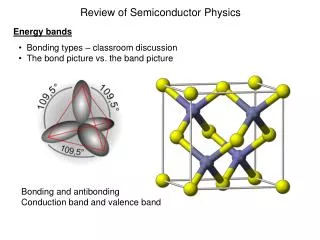
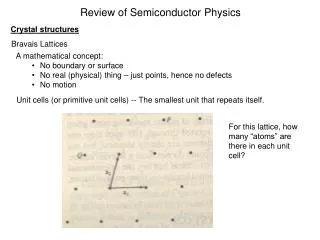
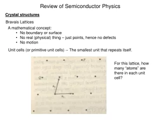
Semiconductor Laser Physics. Wide-gap semiconductor. Narrow-gap semiconductor. Wide-gap semiconductor. E g2. E g1. z. Double Heterojunction. z. E g2. E g1. E g2. Conduction band edge. Valence band edge. Type II. Type I. E c. E c. E g2. E g1. E g2. E g1. E v. E v. Type III.

Semiconductor Laser Physics
E N D
Presentation Transcript
Wide-gapsemiconductor Narrow-gap semiconductor Wide-gap semiconductor Eg2 Eg1 z Double Heterojunction z Eg2 Eg1 Eg2 Conduction band edge Valence band edge
Type II Type I Ec Ec Eg2 Eg1 Eg2 Eg1 Ev Ev Type III Ec Eg1 Ev Ec Eg2 Ev
Evolution of the threshold current of the semiconductor lasers
Basov: Nobel prize 1964 (with Prokhorov and Townes) Basov, Vul, Popov, Krokhin: 1957 first semiconductor laser proposal and development 1961 first injection laser proposal (also Dumke 1962)
The Nobel Prize in Physics 2000 Zhores I. Alferov Herbert Kroemer "for developing semiconductor heterostructures used in high-speed- and opto-electronics"
55 nm Lattice-matched InGaAs/AlInAs
Molecular Beam Epitaxy A. Cho, Bell Labs Needs UHV 10-11 Torr , high-purity elemental materials, right temperature
GaAs/AlxGa1-xAs; GaxIn1-xAsyP1-y/AlxIn1-xAs on InP; InAs1-xSb/AlGa1-xSb on GaSb
Laser waveguides • Vertical confinement • Lateral confinement • Gain-guided • Index guided: ridges, ribs • Buried heterostructure lasers
H-field of the TM00 mode at 8.85 mum In QCLs you can cut the ridge through the active region: strong guiding
Vertical Cavity Surface-Emitting Laser
Edge-emitting laser VCSEL • Large distance between • cavity modes: • – single-mode laser • Circular beam shape • Low threshold and • power consumption • 2D laser arrays • Wafer-scale testing • Ultrafast modulation
For long wavelength laser based on InGaAsP/InP: index contrast is too low, need too many layers, the device is too resistive as a result Current spreading, many transverse modes -> need confinement for current and for the EM field
Oxide aperture Huffaker et al. APL 1994 Problems: different thermal expansion coefficient, strain, bad control, non-planar technology
Phase-shifting mesa Lu et al., APL2004
Oxide aperture and phase-shifting mesa Ahn et al. APL 2005