Download
1 / 46
480 likes | 725 Vues
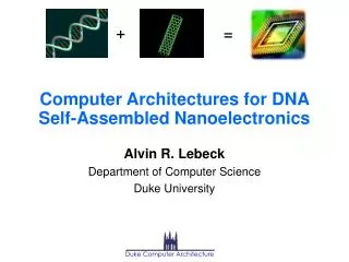
Duke Computer Architecture. +. =. Computer Architectures for DNA Self-Assembled Nanoelectronics. Alvin R. Lebeck Department of Computer Science Duke University. Acknowledgements. People

E N D
Duke Computer Architecture + = Computer Architectures for DNA Self-Assembled Nanoelectronics Alvin R. Lebeck Department of Computer Science Duke University
Acknowledgements People • Students: Jaidev Patwardhan, Constantin Pistol, Vijeta Johri, Sung-Ha Park, Nathan Sadler, Niranjan Soundararajan, Ben Burnham, R. Curt Harting • Chris Dwyer, Daniel J. Sorin, Thomas H. LaBean, Jie Liu, John H. Reif, Hao Yan • Sean Washburn, Dorothy A. Erie (UNC) Funding • Air Force Research Lab • National Science Foundation (ITR) • Duke University Office of the Provost • Equipment from IBM & Intel
Current Processor Designs Large Complex Systems (millions/billions of transistors) Mature technology (CMOS) Precise control of entire design and fabrication process Lithographic process to create smaller and smaller features. But has limits… Cost of facility, high defect rates, process variation, etc. Gate D S Silicon N doped N doped Transistor
The Red Brick Wall • “Eventually, toward the end of the Roadmap or beyond, scaling of MOSFETs (transistors) will become ineffective and/or very costly, and advanced non-CMOS solutions will need to be implemented.”[International Technology Roadmap for Semiconductors, 2003 Edition, Difficult Challenge #10]
The Potential Solution • Self-Assembled Nanoelectronics • Self-assembly • Molecules self-organize into stable structures (nano) • What nanostructures? • What nanoelectronic devices? • How does self-assembly affect computer system design?
Outline • Nanostructures & Components • Circuit Design Issues • Architectural Implications • Proposed Architectures • Defect Tolerance • Conclusion
Sticky End (Tag) 20 nm [Seeman ’99, Winfree et al. ’98,Yan, et al. ’03] DNA Self-Assembly • Well defined rules for base pair matching • Thermodynamics driven hybridization • Can specify sequence of pairs, forms double helix • Synthetic DNA • Engineered Nanostructures • Inexpensive lab equipment (T) Thymine Adenine (A) Cytosine (C) (G) Guanine Strands→Tiles→Structures
DNA-based Self-Assembly of Nanoscale Systems • Use synthetic DNA as scaffolding for nanoelectronics • Create circuits (nodes) using aperiodic patterning • Demonstrated aperiodic patterns with 20nm pitch [FNANO ’05, Angewandte Chemie ’06, DAC ’06]
A C T G Nanoelectronic Components • Many Choices / Challenges • Good Transistor Behavior • Interaction with DNA Lattice • Crossed Nanotube Transistor [Fuhrer et al. ’01] • Demonstrated Functionalization of Tube Ends [Dwyer, et al. ’02] • Other candidates: Ring-gated, Crossed Nanorod, Crossed Carbon Nanotube FETs [Dwyer, et al. IEEE FNANO ’04]
Circuit Design Issues Goal Construct a computing system using the DNA Lattice and nanoelectronic components. Proposal Use DNA tags (sticky-ends) to place nano-components on lattice • Regularity of DNA Lattice • Easy to replicate simple structures on a moderate scale • Complexity of Digital Circuits • Large Graph with many unique nodes and edges • Tolerating Defects • Single-stranded DNA for tags (sticky-ends) may have partial matches (must minimize number of unique tags) • Nanotubes may not work as advertised
20nm Interconnect Layers Vdd plane Ground plane Insulating Layer Balancing Regularity & Complexity A • Array of simple objects • Unit Cell based on lattice cavity • Uniform length nanotubes • Minimizes # of DNA Tags => reduces probability of partial match • 20nm x 20nm • Two levels of interconnect • Complex circuits on single lattice (10K FETS) • Envision ~9µm2 node size: ~10,000 FETs + interconnect • How to get billions or more? B
A B 20nm Self-Assembled System Node Interconnect Node Wire [Yan ’03](selective metallization) + Node • Self-assemble ~ 109 - 1012 simple nodes (~10K FETs) • Potential: Tera to Peta-scale computing • Random Graph of Small Scale Nodes • There will be defects • Scaled CMOS may look similar • How do we perform useful computation?
Outline • Nanostructures & Components • Circuit Design Issues • Architectural Implications • Proposed Architectures • Defect Tolerance • Conclusion
Implications of Small Nodes A • Node: DNA Grid FETs • 3mm x 3mm node • Carbon nanotube [Dwyer ’02] • Ring Gated [Skinner ’05] • Small Scale Control • Controlled complexity only within one node • Limited space on each node • Simple circuits (e.g., full adder) • Limited communication between nodes • only 4 neighbors • No global (long haul) interconnect • Limited coordination • Difficult to get many nodes to work together (e.g., 64-bit adder) B 20nm
Implications of Randomness • Self-assemble interconnect of nodes • Random node placement • Random node orientation • Random connectivity • High defect rates (assume fail stop node) • Limitations -> architectural challenges
Architectural Challenges • Node Design • Utilizing Multiple Nodes • Each node is very simple • Routing • Execution Model • Must overcome implementation constraints • Instruction Set • Micro-scale Interface
Outline • Nanostructures & Components • Circuit Design Issues • Architectural Implications • Proposed Architectures • Defect Isolation & Structure • NANA [JETC ’06] • SOSA [ASPLOS ’06] • Defect Tolerance • Conclusion
Nano-scale Active Network Architecture • Large-scale fabrication (1012 nodes, 109 cells) • Via provides micro-scale interface, Multiple Node Types • First Cut: Understand issues A Single Cell System View
Defect Isolation/Structure • Grid w/ Defects → Random Graph • Reverse path forwarding [Dalal ’78] • Broadcast on all links except input [Nanoarch ’05] • Forward broadcast if not seen before • Implement fail-stop nodes [Nanoarch ’06] • RPF maps out defective regions • No external defect map • Can tolerate up to 30% defective nodes • Distributed algorithm to create spanning tree • Route packets along tree • Up*/down* • Depth first • How do we compute? Anchor Node (after RPF) Defective Node Node Root Direction
NANA: Computing on a Random Graph Exit Enter X - + X X + • Perform 3 operations: Add, Add, Multiply • Search along path for correct blocks to perform function • Execution packets carry operation and values • Proof-of-concept simulations +
A0 B0 C0 D0 B1 C1 D1 NANA: Execution Model & ISA • Accumulator based ISA • Carry data and instructions in a “packet” • Use bit-serial processing elements • Each element operates on one bit at a time • Minimize inter-bit communication opcode Bit Interleaved operands Header op 1 op 2 op 3 A1 A31 B31 C31 D31 Tail
NANA: System Overview • Simple programs • Fibonacci • String compare • Utilization is low • Divide 1012 nodes into 109 cells • Peak performance potentially higher than IBM Blue Gene and NEC Earth Simulator • Need to use more nodes! Log Peak Performance (bitops/sec)
A Control Processor B PE PE 20nm Self-Assembled System Node Interconnect Node Wire [Yan ’03](selective metallization) + Node • Self-assemble ~ 109 - 1012 simple nodes (~10K FETs) • Potential: Tera to Peta-scale computing • Random Graph of Small Scale Nodes • There will be defects • Scaled CMOS may look similar • How do we perform useful computation? • Group many nodes into a SIMD PE • PEs connected in logic ring • Familiar data parallel programming
8 12 5 3 9 6 1 4 10 7 11 2 Self-Organizing SIMD Architecture (SOSA) VIA Tree Edge PE boundary • Nodes Grouped to form SIMD Processing Element (PE) • Head, Tail, N computation nodes (k-wide bit-slice of PE) • Configuration: Depth First Traversal of Spanning Tree • Orders nodes within PE (Head → LSB → …→ MSB → Tail) • Orders PEs • Many SIMD PEs on logical ring → familiar data parallel programming abstraction
SOSA: Instruction Broadcast Enter 8 12 5 PE boundary 3 9 6 1 4 10 7 11 2 • Instructions broadcast to all nodes • Instructions decomposed into three “microinstructions” (opcode, registers, synch) • Can reach nodes/PEs at different times (5 before 9)
SOSA: Instruction Execution Enter 8 12 5 PE boundary 3 9 6 1 4 10 7 11 2 • Instructions execute asynchronously within/across PEs • XOR parallel within PE vs. Addition serial within PE • ISA: Three register operand, predication, optimizations, see paper for details…
One Large System Latency Space sharing Multiple “cells” Throughput Two System Configurations
Outline • Nanostructures & Components • Circuit Design Issues • Architectural Implications • Proposed Architectures • SOSA [ASPLOS ’06] • Node Design • Evaluation • Defect Tolerance • Conclusion
Transceiver 1 C Route Setup Logic VC0 VC0 Buffer Output DeMux Buffer Mux Input Instruction Buffer Transceiver 2 R S Opcode VC1 VC1 Mux Synch Control Reg Buffer Control Output Buffer DeMux Input A L Transceiver 0 U VC2 VC2 Data Buffer Buffer Buffer Output Input Register Specifiers Register File Point to Point Transceiver 3 Route Network Logic Receive Point to Routing Writing Send Logic Virtual Channel 0 Point Logic Entry Logic Channel 1 Channel 2 Virtual Virtual Logic CMD D S D S Logic Analog Control SOSA Node • Homogeneous Nodes • Specialized during configuration • Asynchronous Logic • Communication • 4 tranceivers (4 phase handshake) • 3 virtual channels (inst bcast, ring left & right) • Computation • ALU • Register (32-bits: 32x1 or 16x2) • Inst Buffer • Configuration • Route Setup • Subcomponent BIST [nanoarch ’06]
Transceiver 1 Configuration Logic Transceiver 2 Transceiver 0 Compute Logic Transceiver 3 SOSA Node • VHDL • ~10K FETs • Area ~= 9mm2 • Custom layout tools for standard cells • Power ~= 6.5 W/cm2 • Semi-empirical spice model [IEEE Nano ’04] • 1ns switching time • 88% devices active • 0.775mW / node • Modern proc > 75 W/cm2
Evaluation Methodology • Custom event simulator • Conservative 1ns time quantum (switching time) • 2 bits per node (16 registers, 16 + 2 for 32-bit PE) • Nine benchmarks • Integer code only – no hardware support for floating point • Matrix multiplication, image filters (gaussian, generic, median), encryption (TEA, XTEA), sort, search, bin-packing • Compare performance to four other architectures • Pentium 4 (P4) (real hardware) • ideal out-of-order superscalar (I-SS) 10GHz, 128-wide, 8K ROB • ideal Chip Multiprocessor (I-CMP) 16-way ideal • ideal SOSA (I-SOSA) no communication overhead, unit inst latency • extrapolate for large SOSA systems (back validate)
Matrix Multiply (Execution Time) • Hand optimizations (loop unrolling, etc.) • Better scalability than other systems (crossover < 1000) • Still room for improvement
TEA Encryption (Throughput) • Used in XBOX • shift, add and xor • 64 bit data blocks • 128-bit key • Pipelined on 64 PEs • Configure Multiple Cells of 64 PEs • Single Cell poor • 200X better than P4 in same area
Outline • Nanostructures & Components • Circuit Design Issues • Architectural Implications • Proposed Architectures • Defect Tolerance (not transient faults) • Conclusion
Defect Tolerance Encryption Matrix Multiply • Simple Fail Stop model • Encryption gracefully degrades • MXM < 10% degradation up to 20% defective nodes
Node Failure Modes [Nanoarch ’06] • Exploit modular node design • VHDL BIST for communication & configuration (all stuck-at faults) • Assume software test for compute logic • Configuration logic is critical Transceiver Transceiver Transceiver Configuration Configuration Configuration Transceiver Transceiver Transceiver Compute Logic Compute Logic Compute Logic Transceiver Transceiver Transceiver Transceiver Transceiver Transceiver Compute - Centric Communication - Centric Simple Hybrid – Any Two Components
Evaluation • Simple node model in C • Model network with 10,000 nodes • Vary transistor defect probability from 0%-0.1% • Map defective transistors to defective components • Average 500 runs per data point • How much do we benefit by node modularity? • What device defect probability can it handle?
Results: Usable Nodes • Hybrid failure mode can tolerate a higher device failure probability • Three orders of magnitude greater than typical CMOS designs (10-4 vs. 10-7)
Results: Reachable Nodes • Hybrid increases the number of reachable nodes • More nodes with functioning compute logic reachable and usable
Fail-Stop Summary • Test logic detects defects in node components • Modular node design enables partial node operation • Node is useful if • It can compute OR • It can improve system connectivity • Hybrid failure mode increases available nodes • Can help tolerate a device failure probability of 1.5x10⁻⁴ (1000 times greater than typical CMOS designs)
SOSA Summary • Distributed algorithm for structure & defect tolerance • No external defect map • Configuration groups nodes into SIMD PEs • High utilization w/ familiar programming model • Ability to reconfigure • One system for latency critical systems • Multiple cells for throughput systems • Limitations: I/O bandwidth, general purpose codes, FP, transient faults
+ = Conclusion • Future limits on traditional CMOS scaling • Multicore, etc. -> tera/peta scale w/ 1M nodes • Defects, cost of fabrication, process variation, etc. • High performance, low power despite randomness and defects Engineered DNA Nanostructures Computers Of Tomorrow Nanoelectronics
EA MA 3.3 3.2 3.T 3.1 3.6 3.7 3.0 3.5 3.4 2.6 VIA 3.H 2.7 2.T 1.2 A 2.0 2.1 2.5 1.0 1.1 1.H 1.7 2.2 2.H 1.3 1.5 2.4 1.4 1.6 2.3 1.T Duke Nanosystems Overview DNA Self-Assembly [FNANO 2005, Ang. Chemie 2006, DAC 2006] NANA - General Purpose Architecture [JETC 2006] Logical Structure & Defect Isolation [NANOARCH 2005] Nano DevicesElectronic, optical, etc.[Nanoletters 2006] SOSA - Data Parallel Architecture [NANOARCH 2006, ASPLOS 2006] Large Scale Interconnection [NANONETS 2006] Circuit Architecture [FNANO 2004]
Generic Filter (Execution Time) • 3x3 generic filter (Gaussian & Median similar)
20nm Interconnect Layers Vdd plane Ground plane Insulating Layer Circuit Architecture Carbon nanotubes • Unit Cell based on lattice cavity • Place uniform length nanoelectronic devices • Reduces probability of partial matches • Two layers of interconnect • Achieve balance between • Regularity of DNA lattice • Complexity required for circuits • Defect Tolerance • Node: DNA Lattice with CNFETs Metal nanoparticles
Fail-Stop Transceivers • Minimize test overhead • Reuse node hardware during test • Hardware Test • Send ‘0’ and ‘1’ in a loop • If data returns, enable component • If data does not return, component remains disabled • Similar principle for configuration logic • Modular design enables graceful degradation TEST_OK=0 Test Logic 1 0 0 Transmit Logic Receive Logic Output Buffer Input Buffer Test loopback path