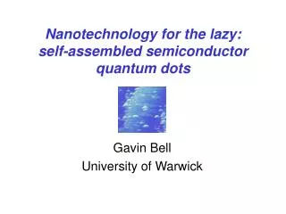
Nanotechnology for the lazy: self-assembled semiconductor quantum dots
330 likes | 644 Vues
Nanotechnology for the lazy: self-assembled semiconductor quantum dots. Gavin Bell University of Warwick. Outline. Semiconductor quantum dots – what, why? Artificial versus self-assembled (SAQD) InAs/GaAs SAQDs Strained heteroepitaxy in MBE Analysing and controlling SAQD growth

Nanotechnology for the lazy: self-assembled semiconductor quantum dots
E N D
Presentation Transcript
Nanotechnology for the lazy:self-assembled semiconductor quantum dots Gavin Bell University of Warwick
Outline • Semiconductor quantum dots – what, why? • Artificial versus self-assembled (SAQD) • InAs/GaAs SAQDs • Strained heteroepitaxy in MBE • Analysing and controlling SAQD growth • STM-MBE versus “STMBE” • SEM, TEM, CAFM
Direct Gap Semiconductors • Direct gap semiconductors: lighting, optical communication, sensors, etc… • For bulk material, the band gap controls the emission wavelength. • Technology sets various ‘target’ wavelengths: • CD player laser 780 nm, DVD 640 nm, Blu-ray and HD-DVD 405 nm. • optical fibre transmission 1300 and 1550 nm.
Low Dimensional Semiconductors • Carriers in electrons can be confined by potential barriers (e.g. in a low gap material surrounded by higher gap material). • Confinement can be in one dimension only – a 2D quantum well. • Confinement in all three directions gives a zero-dimensional quantum dot (QD). • Quantum dot density of states g(E) just discrete levels (no continuum of states – just ‘particle-in-a-box’ energy levels). • Confinement sizes are a few nanometres.
Semiconductor Lasers and LEDs • Various flavours of quantum well lasers – well established technology. • Arakawa and Sakaki (1982) predicted that quantum dot lasers should be more efficient
Real Quantum Dot Lasers • Innolume GmbH • QD lasers 1064 – 1320 nm • QD Laser Inc., Japan • QD lasers 1.3 and 1.55 micro
Artificial Quantum Dots • Nano-fabricated QDs • Position and size control. • Electrical contacting. • Poor quality for optical applications (surfaces and defects cause strong non-radiative recombination). • Hard work! • How about self-assembled QDs?
Molecular Beam Epitaxy • Can we grow 3D / 1D / 0D structures by MBE? • Fire beams of material at substrate crystal in vacuum. • Perfect for growing layer-by-layer (2D) structures. 3D structure (or ‘0D’ if small) 2D structure
Strained Heteroepitaxy • InAs on GaAs leads to 6.7% compressive strain. • 6.7% strain is huge! • Epitaxial stress 5.3 GPa for the (001) surface. • Strain energy in growing layer must be relieved. • Normally: dislocations.
STM-MBE Asx~10-4 Pa STM-MBE Interrupt MBE growth. Transfer pristine surface to STM for atomic-resolution imaging. UHV~10-8 Pa
0.5 ML InAs on GaAs(110) 0.5 ML 2 ML 2 ML STM-MBE (vacuum transfer) 200 nm images. 2D islands then dislocations in 2D layer-by-layer growth. 5 ML
InAs on GaAs(001) 1 ML Regular layer-by-layer growth 2 ML 3D islands Height ~ 3 – 8 nm Width ~ 10 – 20 nm l ~ 10nm, so 0D?
Strain Relief Wetting layer (WL) WL + QDs ε-6.7 % σ5.3 GPa < 1.7 ML > 1.7 ML (very rapid transition) • In-plane strain (epitaxial stress) relieved by 3D islands. • Lattice planes ‘bulge out’. • No dislocations – QDs are coherent. • Balance surface energy against elastic energy.
Control of self-assembly? • Average size & size distribution. • Affects emission wavelength and sharpness. • Density. • Affects gain of QD laser. • Position? • Lateral ordering after many layers. • Don’t need for independent QDs in lasers. • Need to understand growth process.
QD Nucleation GaAs homoepitaxy InAs-GaAs heteroepitaxy islands adatoms 3D island density jumps suddenly at the critical thickness.
In vacuo STM-MBE: Quenching GaAs(001)-(2x4) homoepitaxy 100nm images. ‘Rapid’ quench vs. 10s anneal at the growth temperature: island density drops by 2/3. • Surface rearrangement during quench process? • Cannot return tip to a particular feature to observe its development. • Cannot capture surface dynamics. • QD nucleation extremely rapid – problems?
STMBE versus STM-MBE Asx~10-6 mbar UHV~10-10 mbar STM-MBE The rest of the world!Relatively easy to operate compared to STMBE. STMBE Anan NCT, Japan: Prof. Shiro Tsukamoto.
c b a A 1.70 ML B 1.75 ML QD Nucleation – STMBE Images obtained during growth: 200s per image, corresponds to 0.05 ML coverage interval (0.00025 ML / s). Tip raster direction
A B C Quantum Dot Nucleation – Up Close • Blue arrows: 1 ML height • Red arrows: 3-fold lattice space (1.2 nm) • 3D islands develop over a coverage interval of 0.01 ML. • Total volume in 3D islands jumps from zero to 0.49 ML over a coverage interval of 0.05 ML. • 0.44 ML ‘extra’ In quickly available for QDs.
Wetting Layer Growth • STMBE ‘movie’ of WL growth. • Observe normal step-flow growth. • Fill in pits. • Terrace advances. • Island grows and joins up with terrace. • Each frame 200 s, 0.05 ML. • Measure area of ‘new’ terrace developed in each frame. • Can’t do this with STM-MBE. • Amount of new terrace always less than amount of deposited InAs. • About 0.5 ML In available for rapid QD nucleation as mobile, weakly bound adatoms.
1.6 (2x4) 1.4 (2xa3) 1.2 (1x3) 1.0 increasing (4x2) InAs coverage / ML 0.8 DIFFUSE asymmetry 0.6 0.4 (1xa3) C O E X I S T I N G (2xa3) 0.2 c(4x4) + (1x3) 2 0 c(4x4) ( 2 x 4 ) 350 400 450 500 550 600 Substrate Temperature / °C STMBE: Does the ‘ST’ Interfere With the ‘MBE’? Incommensurate RHEED patterns Direct Fourier transform of STMBE images follow RHEED intensity maxima quite nicely.
QD Composition • Very important in defining potential well (hence optical properties). • STM can’t easily measure composition. • Can infer from cross-sectional STM. • Total QD volume too large for pure InAs QDs. • Must be an InGaAs alloy. • Which technique? • Scanning Transmission Electron Microscopy (Super-STEM). • Grazing incidence X-ray diffraction (synchrotron radiation source). • Medium energy ion scattering (MEIS).
Scanning electron microscopy • SEM • Z-contrast: brighter means more In-rich • QD tops In-rich. • QD bases Ga-rich. • Aligned along steps. • QDs 20-25 nm across. 100 nm
Medium Energy Ion Scattering • UK MEIS facility at Daresbury Laboratories. • Beamline: typically He+ or H+ at 100 keV primary energy. • Toroidal electrostatic analyser records scattered ion energy and angular distributions simultaneously (energy resolution ~ 400 eV). • Able to probe typical samples to a depth of several nm.
Electronic stopping – ion loses energy at a calculable rate (‘stopping power’); these energy losses can be converted to a depth scale. Elastic collision – ion recoils at energy dependent only on scattering angle and mass of target nucleus. Introduction to MEIS surface Align incident beam either along a crystal direction or ‘random’ angle (little channelling hence high counts). Measure the angular and energy spectra of scattered ions. Channelling (lots of low-angle collisions along a crystal direction)
Sample MEIS Data Sample data from two Sb delta-layers in Si. Angular data – crystallographic information (e.g. depth of channelling dip depends on crystalline perfection; e.g. surface structure) Energy spectra – energy resolution best for high mass species in a low mass matrix (e.g. In in GaAs): highest recoil energy. Convert energy scale to depth scale by: energy loss = path length x stopping power Hence produce depth profiles, with near-atomic layer depth resolution.
QD Energy Spectra Channelled spectra, [110] in and normal out, very similar for uncapped (red) and 1 nm GaAs cap (partially capped QDs). Thicker GaAs cap (5 nm): In signal merges into GaAs. Concentrate on uncapped QDs.
Modelling Discrete Structures • MEIS normally applied to 2D layered structures • Every ion recoiling from a particular depth has travelled the same path length. • This is no longer true for discrete structures. • Need to model every possible path through the QD. • Place an average QD on a grid of points and allow ions to enter at each point on the grid. • Energy spectrum is sum over all possible paths. Ion entry point Shallower scattering Deeper scattering
Sample Results for Simulations Simulations for constant In concentration through the QDs (size and density fixed by AFM). Composition is 100% In for the top curve, then 80%, 60%, 40% and 20%. Simulations of linear composition gradient QDs (curves are 0-100% In from bottom to top, 20-100%, 40-100%, 60-100% and 80-100% on each graph).
Best Fit for QDs • Include contributions from QDs, WL and large 3D islands. • Best fit is a linear In gradient from 20% at the QD base to 100% at the QD tops. • The QD bases are rather Ga-rich. • Complex growth kinetics: the WL plays a very important role.
Conclusions • Semiconductor quantum dots. • Self-assembled versus fabricated. • InAs-GaAs QDs easy to grow by MBE. • Possible to tailor to important wavelengths (e.g. 1300 nm). • Study growth in detail with STM. • STMBE ‘movies’ versus STM-MBE ‘snapshots’. • Growth kinetics not fully understood. • Study composition of discrete nanostructures with medium energy ion scattering (MEIS).
Acknowledgments STMBE – Japan: Shiro Tsukamoto, Markus Pristovsek, Brad Orr, Yasuhiko Arakawa, Nobuyuki Koguchi STM-MBE – Imperial College: Tim Jones, Patrick Howe, Tomasz Krzyzewski, Peter Joyce, Azadeh Khatiri, Adam Bone SEM and TEM - Warwick: Richard Beanland, Steve York £££ Royal Society University Research Fellowship ¥¥¥ National Institute for Materials Science – NIMS (Japan) ¥¥¥ Special Coordination Funds (Japanese Government) £££ EPSRC