Power Network Distribution
Power Network Distribution. Chung-Kuan Cheng CSE Dept. University of California, San Diego 11/20/2009. Agenda. Background: power distribution networks (PDN’s) Analysis: worst-case PDN noise prediction Motivation Problem formulation Proposed Algorithm Case study

Power Network Distribution
E N D
Presentation Transcript
Power Network Distribution Chung-Kuan Cheng CSE Dept. University of California, San Diego 11/20/2009
Agenda • Background: power distribution networks (PDN’s) • Analysis: worst-case PDN noise prediction • Motivation • Problem formulation • Proposed Algorithm • Case study • Simulation: adaptive parallel flow using discrete Fourier transform (DFT) • Motivation • Adaptive parallel flow description • Experimental results • Conclusions and future work
Research on Power Distribution Networks • Analysis • Stimulus, Noise Margin, Simulation • Synthesis • VRM, Decap, ESR, Topology • Integration • Sensors, Prediction, Stability, Robustness
Publication List • Power Distribution Network Simulation and Analysis [1] W. Zhang and C.K. Cheng, "Incremental Power Impedance Optimization Using Vector Fitting Modeling,“ IEEE Int. Symp. on Circuits and Systems, pp. 2439-2442, 2007. • [2] W. Zhang, W. Yu, L. Zhang, R. Shi, H. Peng, Z. Zhu, L. Chua-Eoan, R. Murgai, T. Shibuya, N. Ito, and C.K. Cheng, "Efficient Power Network Analysis Considering Multi-Domain Clock Gating,“ IEEE Trans on CAD, pp. 1348-1358, Sept. 2009. [3] W.P. Zhang, L. Zhang, R. Shi, H. Peng, Z. Zhu, L. Chua-Eoan, R. Murgai, T. Shibuya, N. Ito, and C.K. Cheng, "Fast Power Network Analysis with Multiple Clock Domains,“ IEEE Int. Conf. on Computer Design, pp. 456-463, 2007. [4] W.P. Zhang, Y. Zhu, W. Yu, R. Shi, H. Peng, L. Chua-Eoan, R. Murgai, T. Shibuya, N. Ito, and C.K. Cheng, "Finding the Worst Case of Voltage Violation in Multi-Domain Clock Gated Power Network with an Optimization Method“ IEEE DATE, pp. 540-547, 2008. [5] X. Hu, W. Zhao, P. Du, A.Shayan, C.K.Cheng, “An Adaptive Parallel Flow for Power Distribution Network Simulation Using Discrete Fourier Transform,” accepted by IEEE/ACM Asia and South Pacific Design Automation Conference (ASP-DAC), 2010.
Publication List • Power Distribution Network Analysis and Synthesis • [6] W. Zhang, Y. Zhu, W. Yu, A. Shayan, R. Wang, Z. Zhu, C.K. Cheng, "Noise Minimization During Power-Up Stage for a Multi-Domain Power Network,“ IEEE Asia and South Pacific Design Automation Conf., pp. 391-396, 2009. • [7] W. Zhang, L. Zhang, A. Shayan, W. Yu, X. Hu, Z. Zhu, E. Engin, and C.K. Cheng, "On-Chip Power Network Optimization with Decoupling Capacitors and Controlled-ESRs,“ to appear at Asia and South Pacific Design Automation Conference, 2010. [8] X. Hu, W. Zhao, Y.Zhang, A.Shayan, C. Pan, A. E.Engin, and C.K. Cheng, “On the Bound of Time-Domain Power Supply Noise Based on Frequency-Domain Target Impedance,” in System Level Interconnect Prediction Workshop (SLIP), July 2009. [9] A. Shayan, X. Hu, H. Peng, W. Zhang, and C.K. Cheng, “Parallel Flow to Analyze the Impact of the Voltage Regulator Model in Nanoscale Power Distribution Network,” in 10th International Symposium on Quality Electronic Design (ISQED), Mar. 2009.
Publication List (Cont’) • 3D Power Distribution Networks • [10] A. Shayan, X. Hu, “Power Distribution Design for 3D Integration”, Jacob School of Engineering Research Expo, 2009 [Best Poster Award] • [11] A. Shayan, X. Hu, M.l Popovich, A.E. Engin, C.K. Cheng, “Reliable 3D Stacked Power Distribution Considering Substrate Coupling”, in International Conference on Computre Design (ICCD), 2009. [12] A. Shayan, X. Hu, C.K. Cheng, “Reliability Aware Through Silicon Via Planning for Nanoscale 3D Stacked ICs,” in Design, Automation & Test in Europe Conference (DATE), 2009. [13] A. Shayan, X.g Hu, H. Peng, W. Zhang, C.K. Cheng, M. Popovich, and X. Chen, “3D Power Distribution Network Co-design for Nanoscale Stacked Silicon IC,” in 17th Conference on Electrical Performance of Electronic Packaging (EPEP), Oct. 2008. [5] [14] W. Zhang, W. Yu, X. Hu, A.i Shayan, E. Engin, C.K. Cheng, "Predicting the Worst-Case Voltage Violation in a 3D Power Network", Proceeding of IEEE/ACM International Workshop on System Level Interconnect Prediction (SLIP), 2009.
Agenda • Background: power distribution networks (PDN’s) • Analysis: worst-case PDN noise prediction • Motivation • Problem formulation • Proposed Algorithm • Case study • Simulation: adaptive parallel flow using discrete Fourier transform (DFT) • Motivation • Adaptive parallel flow description • Experimental results • Conclusions and future work
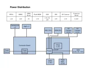
What is a power distribution network (PDN) • Power supply noise • Resistive IR drop • Inductive Ldi/dt noise [Popovich et al. 2008]
PDN Roadmap Vdd of high-performance microprocessors Currents of high-performance microprocessors [ITRS 2007]
PDN Roadmap Target impedance [ITRS 2007]
Agenda • Background: power distribution networks (PDN’s) • Analysis: worst-case PDN noise prediction • Motivation • Problem formulation • Proposed Algorithm • Case study • Simulation: adaptive parallel flow using discrete Fourier transform (DFT) • Motivation • Adaptive parallel flow description • Experimental results • Conclusions and future work
Analysis • Target Impedance vs. Worst Cases • Noise vs. Rise Time of Stimulus • Rogue Wave of Multiple Staged Network
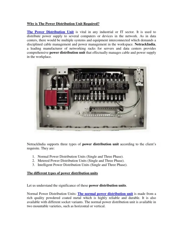
PDN Design Methodology: Target Impedance • PDN design • Objective: low power supply noise • Popular methodology: “target impedance” [Smith ’99] • Implication: if the target impedance is small, then the noise will also be small
Worst-Case PDN Noise Prediction: Motivation • Problems with “target impedance” design methodology • How to set the target impedance? • Small target impedance may not lead to small noise • A PDN with smaller Zmax may have larger noise • Time-domain design methodology: worst-case PDN noise • If the worst-case noise is smaller than the requirement, then the PDN design is safe. • Straightforward and guaranteed • How to generate the worst-case PDN noise FT: Fourier transform
Worst-Case PDN Noise Prediction: Related Work • At final design stages [Evmorfopoulos ’06] • Circuit design is fully or almost complete • Realistic current waveforms can be obtained by simulation • Problem: countless input patterns lead to countless current waveforms • Sample the excitation space • Statistically project the sample’s own worst-case excitations to their expected position in the excitation space • At early design stages [Najm ’03 ’05 ’07 ’08 ’09] • Real current information is not available • “Current constraint” concept • Vectorless approach: no simulation needed • Problem: assume ideal current with zero transition time
Ideal Worst-Case PDN Noise • Problem formulation I • PDN noise: • Worst-case current [Xiang ’09]: Zero current transition time. Unrealistic!
Worst-Case Noise with Non-zero Current Transition Times • Problem formulation II T: chosen to be such that h(t) has died down to some negligible value. * f(t) replaces i(T-τ)
Proposed Algorithm Based on Dynamic Programming • GetTransPos(j,k1,k2):find the smallest i such that Fj(k1,i)≤ Fj(k2,i) • Q.GetMin(): return the minimum element in the priority queue Q • Q.DeleteMin(): delete the minimum element in the priority queueQ • Q.Add(e): insert the element e in the priority queueQ
Proposed Algorithm: Initial Setup • Divide the time range [0, T]into m intervals [t0=0, t1], [t1, t2], …, [tm-1, tm=T]. h(ti) = 0, i=1, 2, …, m-1 • u0 = 0, u1, u2, …, un = b are a set of n+1 values within [0, b].The value of f(t) is chosen from those values. A larger n gives more accurate results. h(t)
Proposed Algorithm: f(t) within a time interval [tj, tj+1] h(t) Theorem 1: The worst-case f(t) can be cons-tructed by determining the values at the zero-crossing points of the h(t) • Ij(k,i): worst-case f(t) starting with uk at time tj and ending with ui at time tj+1
Proposed Algorithm: Dynamic Programming Formulation • Define Vj(k,i): the corresponding output within time interval [tj, tj+1] • Define the intermediate objective function OPT(j,i): the maximum output generated by the f(t) ending at time tj with the value ui • Recursive formula for the dynamic programming algorithm: • Time complexity:
Acceleration of the Dynamic Programming Algorithm • Without loss of generality, consider the time interval [tj, tj+1] where h(t) is negative. • Define Wj(k,i): the absolute value of Vj(k,i): Lemma 1: Wj(k2,i2)- Wj(k1,i2)≤ Wj(k2,i1)- Wj(k1,i1) for any 0 ≤ k1 < k2 ≤ n and 0 ≤ i1 < i2 ≤ n
Acceleration of the Dynamic Programming Algorithm • Define Fj(k,i): the candidate corresponding to k for OPT(j,i) • Accelerated algorithm: • Based on Theorem 2 • Using binary search and priority queue Theorem 2: Suppose k1 < k2, i1∈[0,n]and Fj(k1,i1)≤ Fj(k2,i1), then for any i2 > i1, we have Fj(k1,i2)≤ Fj(k2,i2).
Case Study 1: Impedance 3.23mΩ @ 166MHz 2.09mΩ @ 19.8KHz 1.69mΩ @ 465KHz
Case Study 1: Impulse Response Impulse response: 0s~100ns High frequency oscillation at the beginning with large amplitude, but dies down very quickly Amplitude = 1861 Low frequency oscillation with the smallest amplitude, but lasts the longest Mid-frequency oscillation with relatively small amplitude. Impulse response: 10µs~100µs Impulse response: 100ns~10µs Amplitude = 0.01 Amplitude = 29
Case Study 1: Worst-Case Current • Current constraints: Zoom in • The worst-case current also oscillates with the three resonant frequencies which matches the impulse response. • Saw-tooth-like current waveform at large transition times
Case Study 1: Worst-Case Noise vs. Transition Time • The worst-case noise decreases with transition times. • Previous approaches which assume zero current transition times result in pessimistic worst-case noise.
Case Study 2: Impedance 101.6MHz 98.1MHz 10.9MHz 224.3KHz 224.3KHz 11.2MHz
Case Study 2: Worst-Case Noise • for both cases: meaning that the worst-case noise is larger than Zmax. • The worst-case noise can be larger even though its peak impedance is smaller.
Case 3: “Rogue Wave” Phenomenon • Worst-case noise response: The maximum noise is formed when a long and slow oscillation followed by a short and fast oscillation. • Rogue wave: In oceanography, a large wave is formed when a long and slow wave hits a sudden quick wave. High-frequency oscillation corresponds to the resonance of the 1st stage Low-frequency oscillation corresponds to the resonance of the 2nd stage
Case 3: “Rogue Wave” Phenomenon (Cont’) Equivalent input impedance of the 2nd stage at high frequency
Case 3: “Rogue Wave” Phenomenon (Cont’) V2nd V2nd_only
Case 3: “Rogue Wave” Phenomenon (Cont’) IL2 IL1 IL
Case 3: “Rogue Wave” Phenomenon (Cont’) Zoom in IL2 IL1 IL
Case 3: “Rogue Wave” Phenomenon (Cont’) V2nd V1st-V2nd V1st_only
Case 3: “Rogue Wave” Phenomenon (Cont’) Zoom in V2nd V1st-V2nd V1st_only
Case 3: “Rogue Wave” Phenomenon (Cont’) max(V1st)=37.34mV V2nd V1st V1st-V2nd max(V2nd_only) + max(V1st_only) = 42.09mV ≈ max(V1st) V2nd_only V1st_only
Agenda • Background: power distribution networks (PDN’s) • Analysis: worst-case PDN noise prediction • Motivation • Problem formulation • Proposed Algorithm • Case study • Simulation: adaptive parallel flow using discrete Fourier transform (DFT) • Motivation • Adaptive parallel flow description • Experimental results • Conclusions and future work
PDN Simulation: Why Frequency Domain? • Huge PDN netlists • Time-domain simulation: serial - slow • Frequency-domain simulation: parallel – fast • Frequency dependent parasitics • Simulation results • Time-domain: voltage drops, simultaneous switching noise (SSN) – input dependent • Frequency-domain: impedance, anti-resonance peaks – input independent
Transform Operations • Laplace Transform [Wanping ’07] • Input: Series of ramp functions • Output: Rational expressing via vector fitting • Choice of frequency samples • Discrete Fourier Transform (DFT) • Periodic signal assumption • Discrete frequency samples
Adaptive DFT Flow • Period[i]: the input period at each iteration • Interval[i]: the simulation time step at each iteration • FreqUpBd[i]: the upper bound of the input frequency range at each iteration • vi(t): tentative time-domain output within the frequency range [0, FreqUpBd] at each iteration • Iteration #1: obtain the main part of the output • Iteration #2~k: capture the oscillations in the tail of the output (high, middle, and low resonant frequencies) • For each iteration #i, i=k, k-1, …, 2, subtract the captured tail from the outputs at iteration #j, j<i to eliminate the wrap-around effect
Problem with Basic DFT Flow • “Wrap-around effect” requires long padding zeros at the end of the input • Periodicity nature of DFT • Small uniform time steps are needed to cover the input frequency range T 2T 3T 4T T Large number of simulation points! Correct output T Wrap-around DFT repetition Distorted! output
Adaptive DFT Simulation T 2T 3T 4T T - • Basic ideas of the adaptive DFT flow: cancel out the wrap-around effect by subtracting the tail from the main part of the output • Main part of the output: obtained with small time step and small period; distorted by the wrap-around effect • Tail of the output: low frequency oscillation; can be captured with large time steps - - Correct! Correct Distorted Total number of simulation points is reduced significantly!
Experimental Results: Test Case & Input • Test case: 3D PDN • One resonant peak in the impedance profile • Input current • Time step: ∆t = 20ps • Duration: T0 = 16.88ns Original Input Impedance
Experimental Results: Adaptive Flow Process T1 • Iteration #1: v1(t) • ∆t1=20ps • T1=20.48ns • Iteration #2: v2(t) • ∆t2 = 32∆t1 = 640ps • T2 = 4T1 = 81.92ns • Final output: • Main part: • Tail: v1(t), ∆t1=20ps, T1=20.48ns 3T1 2T1 4T1 v2(t), ∆t2=640ps, T2=81.92ns Final output
Error Analysis: Error Caused by Wrap-around Effect Output comparison Error relative to SPICE Relative error: 0.12% Relative error: 2.09% Theorem 1: Let be the initial value of the output voltage. Suppose for some , then the mean square error, i.e., is bounded by .