New high resolution spectrometer for nanometer level elemental depth profiling
This paper presents a newly developed high-resolution spectrometer designed for nanometer-level elemental depth profiling. Utilizing Time-of-Flight Elastic Recoil Detection (ToF-ERD), the spectrometer achieves exceptional timing and energy resolution, enabling the quantification of all sample elements, including hydrogen. The system demonstrates a depth resolution of less than 2 nm and excellent detection efficiency for various masses, paving the way for enhanced material characterization in research and industry. Future enhancements are expected to further optimize its capabilities.

New high resolution spectrometer for nanometer level elemental depth profiling
E N D
Presentation Transcript
New high resolution spectrometerfor nanometer levelelemental depth profiling M. Laitinen, M. Rossi, P. Rahkila, H. J. Whitlow and T. Sajavaara Department of Physics, P.O.B 35, FIN-40014 University of Jyväskylä, Finland email: mikko.i.laitinen@jyu.fi
The New Spectrometer:What does it look like and how does it works ?
The new spectrometer:How does it look like and how it works ? • In principleallsampleelementscanbequantified M. Putkonen, T. Aaltonen, M. Alnes, T. Sajavaara, O. Nilsen, and H. Fjellväg, Atomic layer deposition of lithium containing thin films, J. Mater. Chem. 19 (2009) 8767.
Time-of-Flight – Elastic Recoil Detection (ToF-ERD) • Quantitative method: • Energy from well known kinematics • Time-resolution better than E-detector resolution • Element (mass) from ToF and E signals • Scattering propability to detectors • Coulombic interaction potential • Depth information • Semi-empiric parametrization for energy loss
TOF detection efficiency • All sample elements, also H, can be detected • Can get better only by getting more electrons out of the carbon foils • -> coating the carbon foils with Atomic Layer Deposition, ALD • Better than 98% for C • and heavier masses • ~ 90 % for 4He • ~ 10-60% for H Sample holder backwall Measured with 1600 V MCP voltage, 3000 V mirror voltage and 200x preamplifier
Time-of-flight resolution • Timing with external 200x preamplifier, CFD and TDC • Current resolution timing resolution 300 ps for 4.5 MeV incident He ions scattered from 1 nm Au film on Si substrate • Timing:300 ps equals ~ 4mm for 4.4 MeV He • Upgrade:fastpreamplifiers inside the chamber 300 ps
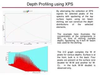
Diamond-like carbon films • 2.3 µm thick diamond-like-carbon film on Si • Measured with 9 MeV 35Cl • All isotopes can be determined for light masses • Light elements can be well quantified (N content 0.05±0.02 at.%)
First results: 8.6 nm Al2O3 • Atomic layer deposited Al2O3 film on silicon (Prof. Ritala, U. of Helsinki) • Density of 2.9 g/cm3 and thickness of 8.6 nm determined with XRR (Ritala) • Elemental concentrations in the film bulk as determined with TOF ERDA are O 60±3 at.%, Al 35±2 at.%, H 4±1 at.%. and C 0.5±0.2 at.%.
Example with high mass element • AtomiclayerdepositedRufilm on HF cleanedSi(Dr. Kukli, U. of Helsinki) • Bulkdensity of 12 g/cm3used in the depthprofiles • Monte Carlo simulationsneeded for gettingreliablevalues for lightimpurities
Future improvements: New TOF-gate • ALD-coated thin C-foils for high electron yields (coming) • Timing from backwards emitted electrons • Position (scattering angle) from forward emitted electrons and delay line anode • Anodes made on PCB Commercial MCP stacksby TECTRA
Future improvements: Gas ionization detector TOF-E results from Paul Scherrer Institute Incident ion 12 MeV 127I and borosilicate glass target Nucl. Instr. and Meth. B248 (2006) 155-162
Conclusions • New high resolution spectrometer has been built in JYFL • ToF-ERDA provides unique capabilities for quantitative depth profiling of all the sample elements, including hydrogen • Depth resolution of <2 nm at the surface has been reached in Jyväskylä, further improvements coming within months 2nd timing detector, 10 μg/cm2 C-foil 1st timing detector, 3 μg/cm2 C-foil
Acknowledgements Mikko Ritala, U. of Helsinki Matti Putkonen, Beneq Oy and Aalto University Kaupo Kukli, U. of Helsinki TEKES-EU Regional Funds Academy of Finland TEKES Accelerator based materials physics goup in JYFL
1st timing detector, 3 μg/cm2 C-foil 2nd timing detector, 10 μg/cm2 C-foil