Example 1: Equilibrium PN-Junction
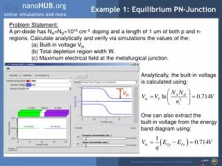
Example 1: Equilibrium PN-Junction. Problem Statement: A pn-diode has N A =N D =10 16 cm -3 doping and a length of 1 um of both p and n-regions. Calculate analytically and verify via simulations the values of the: (a) Built-in voltage V bi (b) Total depletion region width W.

Example 1: Equilibrium PN-Junction
E N D
Presentation Transcript
Example 1: Equilibrium PN-Junction Problem Statement: A pn-diode has NA=ND=1016 cm-3 doping and a length of 1 um of both p and n-regions. Calculate analytically and verify via simulations the values of the: (a) Built-in voltage Vbi (b) Total depletion region width W. (c) Maximum electrical field at the metallurgical junction. Analytically, the built-in voltage is calculated using: Vbi One can also extract the built-in voltage from the energy band diagram using:
Example 1: Charge Density W Question1: What is the analytical value of the total depletion region width? Answer1: The analytical value of the depletion region width is 0.432 um. Question2: What is the extracted simulated value of the total depletion region width? Answer2: The simulated value of the depletion region width is ~ 0.43 um.
Example 1: Electric Field Profile Emax Question1: What is the analytical value of the peak electric field? Answer1: The analytical value of the peak electric field is 33.14 kV/cm. Question2: What is the extracted simulated value of the peak electric field? Answer2: The simulated value of the peak electric field is 32 kV/cm.
Example 2: PN-Junction Under Bias Problem Statement: A pn-diode has NA=ND=1016 cm-3 doping and a length of 1 um of both p and n-regions. Simulate: (a) Energy band profile under applied bias VA=0.6 V (b) quasi-Fermi level variation with position (c) electric field under bias (d) forward IV-characteristic of the diode The net built-in voltage is: Vbi - VA = 0.714 -0.6 = 0.114 V The value extracted from the graph for the net built-in voltage is 0.115 V.
Example 2: Quasi-Fermi Level Variation Question: Where is the variation of the quasi-Fermi levels significant? Answer: The variation of the quasi-Fermi levels is significant in regions in which the carrier concentration changes by orders of magnitude.
Example 2: Electric Field Under Bias Question1: Compare the equilibrium and non-equilibrium values of the field! Answer1: The peak non-equilibrium field is lower. Question2: Compare the equilibrium and nonequilibrium depletion region widths! Answer2: The non-equilibrium depletion region with is smaller under forward bias.
Example 2: Current Density Question: How does the current vary with increasing the doping density of either the p- or n-region, or both? Answer: With increasing the doping density of either the p-side, or the n-side, or both, the potential barrier for the minority carriers increases and the current decreases.
Example 3: Non-Symmetric Junction Problem Statement: A pn-diode has NA=1016 cm-3 and ND=1018 cm-3 doping, and a length of 1 um of both p and n-regions. Simulate: (a) equilibrium energy band profile (b) charge density, to see the extent of the depletion regions (c) electric field profile to examine the contribution of the inversion charge
W Example 3: Charge Density Question1: What is the analytical value of the total depletion region width? Answer1: The analytical value of the depletion region width is0.327 um. Question2: What is the extracted simulated value of the total depletion region width? Answer2: The extracted simulated value of the depletion region width is ~ 0.31 um.
Example 3: Electric Field Profile Inversion charge Depletion charge Question1: What is the analytical value of the peak electric field? Answer1: The analytical value of the peak electric field is 50.2 kV/cm. Question2: What is the extracted simulated value of the peak electric field? Answer2: The simulated value of the peak electric field is 67.1 kV/cm.
Example 4: Series Resistance Problem statement: In this exercise we will examine the series resistance effects under high bias conditions. The p-side doping is NA=1016 cm-3 and the n-side doping is ND=1016 cm-3. The length of the p-side and the n-side region is taken to be 1 um. Plot the following variables: (a) Conduction band, valence band and the intrinsic level variation vs. position for applied bias VANODE=1.2 V. (b) Quasi-Fermi level variation. (c) Forward IV-characteristics of a diode for applied bias between 0 and 1.2 V in 0.05 V increments. From the forward IV-characteris- tics under high bias conditions extract the series resistance.
Example 4: Current Density Series resistance effect Ideal characteristics
V1 V2 Example 4: Current Density, Cont’d The ideal diode current is The non-ideal diode current is: V=V2-V1=RID => R= V/ID From the equality of the currents we have: