Process-Variation Tolerant Design Techniques for Multiphase Clock Generation
Process-Variation Tolerant Design Techniques for Multiphase Clock Generation. Manohar Nagaraju + , Wei Wu*, Cameron Charles # + University of Washington, Seattle, WA, USA # University of Utah, Salt Lake City, UT, USA *Northwestern Polytechnic University, Xi ’ an, China. Outline.

Process-Variation Tolerant Design Techniques for Multiphase Clock Generation
E N D
Presentation Transcript
Process-Variation Tolerant Design Techniques for Multiphase Clock Generation ManoharNagaraju+, Wei Wu*, Cameron Charles# +University of Washington, Seattle, WA, USA #University of Utah, Salt Lake City, UT, USA *Northwestern Polytechnic University, Xi’an, China
Outline Background on clock and data recovery (CDR) and motivation Circuit level and system level optimization Measurement results Conclusion
Motivation Increasing I/O bandwidth complicates CDR circuit design, particularly the VCO Solution: over-sample the incoming data
Motivation Use a Delay-Locked Loop (DLL) to recover data at N*clock frequency
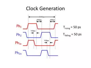
Motivation Non-Ideal Sampling Ideal Sampling Input Data • Problems in multiphase clock generation • Mismatch in delay among delay blocks • Overall frequency controlled by loop but phase relationships uncontrolled
Motivation Delay Distribution of inverter pair Vt mismatch of 100mV • Sources of mismatch • Mismatch in Vt • Mismatch in W/L
Motivation • Delay of stage 1: 686.3ps • Delay of stage 2: 695.5ps • Delay of stage 3: 695.5ps • Delay of stage 4: 654.5ps • Sources of mismatch • Mismatch in Vt • Mismatch in W/L • Mismatch in load
Solution Propose circuit-level design methodology to reduce mismatch Introduce extra control on the individual phases – digital calibration
Circuit-level optimization A transistor sizing scheme to reduce mismatch Expression for variable of interest (here delay) as a function of process parameter (here Vt) Differentiate w.r.t process parameter Design circuit to ensure the resulting expression is small
Circuit-level optimization • Ex: A CMOS inverter • Fall time: • Following procedure, length should be increased
Circuit-level optimization Increase W/L Reduce W/L Increase W/L Increase W/L Schematic of a single delay cell
Circuit optimization results • Optimized • co-efficient of variation = 3.05% • b) Un-optimized • co-efficient of variation = 6.73% Monte-Carlo simulation
Limitation VCDL gain becomes non-linear
Limitation VCDL gain becomes non-linear Lock range of DLL reduces 0.5 Trefclk< T VCDL, min < Trefclk Trefclk< TVCDL max < 1.5 * T ref clk Process complicated with the number of variables increasing Delay still varies from 205-250 ps (5.57˚) – quite large for multiphase clocking scheme
Phase control by digital calibration Based on equation fring_osc = (1/2NTd)
Calibration of the VCDL • Difference between ring oscillator frequencies indicates difference in delays • To change delay of delay block • Change Vt - requires DAC • Change current which is the parameter of interest – by changing widths dynamically
Calibration of the VCDL • Modify delay cell • Resolution = 9.8ps • Delay variation • -140ps
Die photo AMI 0.6um CMOS process - 2300um X 900um
Measurement results Lock range – 185-240MHz Power: 15.4mA + 46.4mA (calibration) Time required for calibration 8.29us.
Measurement results 3.28˚ 1.09˚ 0.4˚ Delay values of the four delay blocks before and after calibration at 227MHz
Summary • Proposed a new methodology to design process-invariant circuits • Proposed a digital calibration scheme to reduce mismatches in delay • Maximum phase offset among delay blocks was reduced to 1.09°
Thank You