8x LVDS on HDMI
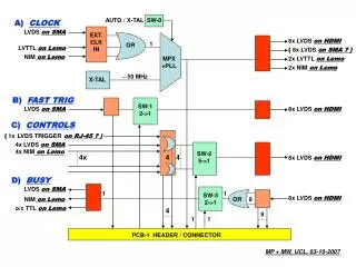
AUTO / X-TAL. SW-0. A) CLOCK. LVDS on SMA. EXT.CLKIN. 8x LVDS on HDMI. 1. OR. LVTTL on Lemo. ( 8x LVDS on SMA ? ). NIM on Lemo. MPX +PLL. 2x LVTTL on Lemo. 2x NIM on Lemo. ~ 50 MHz. X-TAL. B) FAST TRIG. SW-1 2->1. LVDS on SMA. 8x LVDS on HDMI. C) CONTROLS.

8x LVDS on HDMI
E N D
Presentation Transcript
AUTO / X-TAL SW-0 A) CLOCK LVDS on SMA EXT.CLKIN 8x LVDS on HDMI 1 OR LVTTL on Lemo ( 8x LVDS on SMA ? ) NIM on Lemo MPX +PLL 2x LVTTL on Lemo 2x NIM on Lemo ~ 50 MHz X-TAL B) FAST TRIG SW-1 2->1 LVDS on SMA 8x LVDS on HDMI C) CONTROLS ( 1xLVDS TRIGGERon RJ-45 ? ) 4x LVDS on SMA 4x NIM on Lemo SW-2 5->1 4x 4 4 8x LVDS on HDMI D) BUSY LVDS on SMA 1 1 SW-3 2->1 8x LVDS on HDMI NIM on Lemo OR 8 o/c TTL on Lemo 4 8 1 1 PCB-1 HEADER / CONNECTOR MP + MW, UCL, 03-10-2007
CALICE C&C PROPOSAL - DRAFT -4-FOR COMMENTS & CORRECTIONS A) CLOCK : a) 3x EXTERNAL INPUTS : 1) 1x Diff. LVDS ( 2x SMA ) 2) 1x LVTTL/CMOS (?) ( 1x Lemo 00 ) 3) 1x NIM ( 1x Lemo 00 ) b) INTERNAL X-TAL OSCILLATOR ( 100MHz clk ) - Inputs a1+a2+a3 converted to single-ended LVTTL/CMOS (?) level All three plain OR-ed together to produce single EXT-CLK-IN b) output divided-by-two to produce INT-CLK at 50MHz, LVTTL/CMOS (?) - EXT-CLK-IN and INT-CLK input into Mux-PLL ( ICS581 ? ) to produce single clock CLK-OUT, automatically switching from EXT-CLK-IN to INT-CLK if external clock missing for > 3 periods - Hardware switch SW-0 to force Mux. to switch to 50MHz INT-CLK input - Mux-PLL output : 45min/55max Duty Cycle +/- 150ps max absolute period jitter CLK-OUT OUTPUTS : 1) 8/10/12x Diff. LVDS outputs ( on HDMI each ) 2) [ 8/10/12x Diff. LVDS outputs ( 2x SMA each ) ?? ] 3) 2x LVTTL/CMOS (?) ( 1x Lemo 00 each ) 4) 2x NIM ( 1x LEMO 00 each ) 5) 1x Diff. LVDS on PCB-1 Header ( see below )
B) FAST TRIGGER : 1x FAST TRIGGER INPUT : 1x Diff. LVDS ( 2x SMA ) - Input B1) passed straight onto a dual rotary-selector switch or header/jumper selector SW-1 - Input B1) passed also onto the PCB-1 Header as 1x Diff. LVDS output ( see below ) 8/10/12x FAST TRIGGER OUTPUTS : 1) 8/10/12x Diff. LVDS outputs ( on HDMI each ) produced from the output of the selector SW-1 from either the Input A or from Input AP on the PCB-1 Header ( see below ) C) CONTROLS : c) 3x EXT. TRIGGER INPUTS : 1) 1x Diff. LVDS ( 2x SMA ) 2) 1x NIM ( 1x Lemo 00 ) 3) [ 1x Diff. LVDS ( 1x PJ-45 ) ?? ] d) 2x EXT. START INPUTS : 1) 1x Diff. LVDS ( 2x SMA ) 2) 1x NIM ( 1x Lemo 00 ) e) 2x EXT. AUX-1 INPUTS : 1) 1x Diff. LVDS ( 2x SMA ) 2) 1x NIM ( 1x Lemo 00 ) f) 2x EXT. AUX-2 INPUTS : 1) 1x Diff. LVDS ( 2x SMA ) 2) 1x NIM ( 1x Lemo 00 ) - Each set of Inputs c1+c2+c3, d1+d2, e1+e2, f1+f2 are OR-ed together, producing single-ended signals c12, d12, f12. f12 - Each line c12, d12, e12, f12 ends with rotary-selector switch or header/jumper selector SW-2 - Each line c12, d12, e12, f12 passed also onto the PCB-1 Header as single-ended outputs ( see below ) 8/10/12x CONTROL OUTPUTS : 1) 8/10/12x Diff. LVDS outputs ( on HDMI each ) - produced from the output of the selector SW-2 from either the four inputs c12, d12, e12, f12 or from single Input CONTROL-P on the PCB-1 Header ( see below )
D) BUSY FEEDBACK : 8/10/12x BUSY FEEDBACK INPUTS : 1) 8/10/12x Diff. LVDS ( on HDMI each ) - All 8/10/12x inputs sent to the PCB-1 Header ( see below ), as well as being all OR-ed with the single output BUSY sent to a switch-selector or header/jumper SW-3 ( see below ) 3x BUSY OUTPUTS : 1) 1x Diff. LVDS ( 2x SMA ) 2) 1x NIM ( 1x Lemo 00 ) 3) 1x o/collector TTL ( 1x Lemo 00 ) - BUSY OUTPUTs produced from the output of the selector SW-3 from either the single BUSY input or from single input BUSY-P on the PCB-1 Header ( see below ) PCB-1 HEADER : standard 0.1" dual PCB Header to provide connections to a control/ODR PCB for possible processing of signals on FPGA PCB-1 Header carries the following lines : - one pair Diff. LVDS line CLK-OUT output - one pair Diff. LVDS line A Fast Trigger output - one pair Diff. LVDS line AP Fast Trigger input - four c12, d12, e12, f12 single-ended CONTROL outputs - one single-ended CONTROL-P input - 8/10/12 single-ended BUSY-N outputs - one single-ended BUSY-P input POWER : It is proposed to have an external P/S, connected to the C&C PCB by a DC power socket