Feedback Amplifiers in Electronic Circuits
510 likes | 726 Vues
Explore how feedback amplifiers work, types of feedback effects, unit analysis, feedback topologies, and gain stabilization techniques. Learn about the Nyquist criterion, gain/phase margins, and oscillator mechanisms for stable circuits.

Feedback Amplifiers in Electronic Circuits
E N D
Presentation Transcript
Electronic circuits-II EC2251
Unit-1 Feedback amplifiers
Feedback • Consists of returning part of the output of a system to the input • Negative Feedback: a portion of the output signal is returned to the input in opposition to the original input signal • Positive Feedback: the feedback signal aids the original input signal • Negative Feedback Effects: • Reduces gain • Stabilizes gain • Reduces non linear distortion • Reduces certain types of noise • Controls input and output impedances • Extends bandwidth • The disadvantage of reducing the gain can be overcome by adding few more stages of amplification
Af--- closed loop gain A---Open loop gain A----loop gain Feedback amplifier. Note that the signals are denoted as xi, xf, xo, and so on. The signals can be either currents or voltages Negative feedback(Af<A) Positive feedback (Af>A) Positive feedback provides an easy way to obtain large gain. It leads to poor gain stability , a slight shift in power supply Or temp can change the magnitude of loop gain to unity & cause the Amplifier to break into oscillation .
Types of Feedback There are 4 basic types of feedback that have different effects: • Voltage series • Current series • Voltage shunt • Current shunt The units of are the inverse of the units of the amplifier gain • For series-voltage feedback A=Av and is unit less • For series-current feedback A=Gm and is in W • For voltage shunt feedback A=Rm and is in Siemens • For current shunt feedback A=Ai and is unit less
The four basic feedback topologies: (a) voltage-sampling series-mixing (series-shunt) topology; (b) current-sampling shunt-mixing (shunt-series) topology; (c) current-sampling series-mixing (series-series) topology; (d) voltage-sampling shunt-mixing (shunt-shunt) topology.
Effects of various types of feedback on gain Gain Stabilization • If we design the amplifier so that Ab >> 1, then the closed loop gain Af is approximately 1/b • Under this condition Af depends only on the stable passive components (resistor or capacitors) used in the feedback network, instead of depending on the open loop gain A which in turn depends on active device parameters (gm) which tend to be highly variable with operating point and temperature
Analysis of feedback amplifiers Steps 1.Identify the type of feedback 2.Redraw the amplifier circuit without the effect of feedback . 3.Use a thevenin’s source at the input for series mixing and use a Norton’s source at the input for shunt mixing. 4.After drawing the amplifier circuit without feedback determine the ac parameters of the circuit using the h parameter model. 5.Determine the feedback ratio b = xf / xo from the original circuit. 6. Find he desensivity factor(D). 7.Knowing A,D,Ri,and Ro , Find Af, Rif , Rof.
Nyquist criterion Criterion Of Nyquist: The amplifier is unstable if this curve encloses the point –1+j0 and the amplifier is stable if the curve does not enclose this point Im(A) fn A Re (A) Gain and phase margins • These are a measureof the stability of acircuit -1+j0 1+ A f2 f1
Unit -2 Oscillator
Oscillators are circuits that produce a continuous signal of some type without the need o an input. • These signals serve a purpose for a variety of purposes. Communications systems, digital systems (including computers), and test equipment make use of oscillators. • An oscillator is a circuit that produces a repetitive signal from a dc voltage. • The feedback type oscillator which rely on a positive feedback of the output to maintain the oscillations. • The relaxation oscillator makes use of an RC timing circuit to generate a non-sinusoidal signal such as square wave.
The requirements for oscillation are described by the Baukhausen criterion: • The magnitude of the loop gain A must be 1 • The phase shift of the loop gain A must be 0 or 360 or integer multiple of 2pi
Amplitude stabilisation • in both the oscillators above, the loop gain is set by component values • in practice the gain of the active components is very variable • if the gain of the circuit is too high it will saturate • if the gain of the circuit is too low the oscillation will die • real circuits need some means of stabilising the magnitude of the oscillation to cope with variability in the gain of the circuit Mechanism of start of oscillation: • The starting voltage is provided by noise, which is produced due to random motion of electrons in resistors used in the circuit. • The noise voltage contains almost all the sinusoidal frequencies. This low amplitude noise voltage gets amplified and appears at the output terminals. • The amplified noise drives the feedback network which is the phase shift network. Because of this the feedback voltage is maximum at a particular frequency, which in turn represents the frequency of oscillation.
RC or phase-shift oscillator • one way of producing a phase shift of 180 is to use an RC ladder network • this gives a phase shift of 180 • at this frequency the gain of the network is
Wien-bridge oscillator • uses a Wien-bridge network • this produces a phase-shiftof 0 at a single frequency, and is used with an invertingamplifier • the selected frequency is fr = 1/2RC • when the gain is 1/3
Twin T Oscillator The twin-T utilizes a bandstop arrangement of RC circuits to block all but the frequency of operation in the negative feedback loop. The only frequency allowed to effectively oscillate is the frequency of resonance.
The Colpitts oscillator utilizes a tank circuit (LC) in the feedback loop. Since the input impedance affects the Q, an FET is a better choice for the active device. fr = 1/2LCT The Clapp is similar to the Colpitts with exception to the additional capacitor in the tank circuit.
The Hartley oscillator is similar to the Clapp and Colpitts. The tank circuit has two inductors and one capacitor. • Frequency of oscillation
The Armstrong oscillator uses transformer coupling in the feedback loop. For this reason the Armstrong is not as popular.
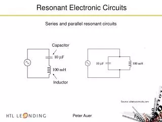
Crystal oscillators An oscillator in which the frequency is controlled by a piezoelectric crystal. A crystal oscillator may require controlled temperature because its operating frequency is a function of temperature • frequency stability is determined by the ability of the circuit to select a particular frequency • in tuned circuits this is described by the quality factor, Q • piezoelectric crystals act like resonant circuits with a very high Q – as high as 100,000
Unit-3 Tuned Amplifiers
Tuned Circuits • Frequency selectivity of resonant circuits allows a radio to be tuned to one of a set of transmitting stations. • Tuning is usually undertaken by varying the capacitance of an adjustable capacitor. • Resonant circuits are also important for tuning and for transmitting signals. Tuned amplifiers • To amplify the selective range of frequencies , the resistive load , Rc is replaced by a tuned circuit. • The tuned circuit is capable of amplifying a signal over a narrow band of frequencies centered at fr.
Types Of tuned amplifiers Single tuned amplifier • one parallel tuned circuit is used as a load • Limitation: Smaller Bandwidth , smaller gain bandwidth product, does not provide flatten response. Double tuned amplifier • It provides high gain, high selectivity and required bandwidth. • Used in IF in radio and TV receivers. • It gives greater 3db bandwidth having steep sides and flat top . But alignment of double tuned amplifier is difficult Stagger tuned amplifier • Two single tuned amplifier are connected in cascaded form. • Resonant frequency are displaced. • To have better flat , wideband charcteristics with a very sharp rejective, narrow band characteristics.
Synchronously tuned amplifier • To obtain a high over all gain , several identical stages of tuned amplifiers can be used in cascade. • All amplifiers stages are assumed to be identical and to be tuned to the same frequency w0. Q factor: • Ratio of reactance to resistance. • Measure of efficiency with which inductor can store the energy. Unloaded Q of tuned circuit • Ratio of stored energy to dissipated energy in a reactor or resonator. Loaded Q • It is determined by how tightly the resonator is coupled to its terminations.
Instability of tuned circuits • Transistor are used at the frequencies nearer to their unity gain BW to amplify narrow band of high frequencies. • At this RF frequencies , inter capacitance between base and collector becomes dominant. • Some feedback signal manages to reach the input from output , so circuit becomes unstable and generating the oscillation and can stop working as amplifier. Stabilization techniques: • Hazeltine neutralization • Neutrodyne neutralization • Neutralization using coil • Rice neutralization
Class C amplifiers • Class C amplifiers cannot be used in audio circuitry because of their high distortion. • Class C amplifiers can be used as tuned rf amplifiers where the undesired harmonic frequencies can be filtered out. • A class C amplifier is more efficient than either a class A or class B amplifier; its efficiency approaches 100%. • The input coupling capacitor, base resistor, and base-emitter junction form a negative clamper. • Because of the clamping action, only the positive peaks of the input signal drive the transistor, Q1, into conduction. • The RBC time constant is made long with respect to the period of the input waveform to provide the proper clamping action.
Equivalent input circuit of class c TUNED AMPLIFIER • At the resonant frequency, fr, the impedance of the tuned LC circuit is maximum. • The tank impedance, Ztank, is purely resistive at fr. Application: used in radio receivers ad mixer circuits.
Unit-4 Blocking Oscillator
Linear wave shaping :Process by which the shape of a non sinusoidal signal is changed by passing the signal through the network consisting of linear elements • Diodes can be used in wave shaping circuits. • Either limit or clip signal portion--- clipper shift the dc voltage level of the signal --- clampers • Types of non sinusoidal input step, pulse ,square, Ramp input
RC circuits (Step Response) Low-Pass High-Pass Vin Vout Vin Vout Vin Vin Vout Vout Voltage on capacitor cannot change instantaneously. So Vout = Vin initially. Voltage on capacitor cannot change instantaneously. So Vout = 0 initially.
L=1 mH Vout ~ R Vin RL circuit RL circuit is used for small time constants. To get a large time constant the inductance value has to be chosen high Higher inductance value are provided by iron core inductors which are bigger in size, heavy and costly.
Fall Time & Time Constant Relationship Between Time Constant T & Rise-Time or Fall-TimeT = RC or L/R Rise-Time (Fall-Time) = T X ln9 = 2.2T Vout 100% 1.0 0.9 90% 1/e~37% 10% 0.1 time Fall Time
Clippers • Clipping removes part of the positive or negative peaks of a signal or both. Silicon diodes do not conduct until the applied voltage exceeds about 0.6 volts and only when the anode is positive with respect to the cathode. • The circuit is like a potential divider with the diode part being high resistance for voltages below 0.6 volts and low resistance above.
During the negative half cycle of the input signal, the diode conducts and acts like a short circuit. • The output voltage Vo 0 volts . The capacitor is charged to the peak value of input voltage Vm. and it behaves like a battery. • During the positive half of the input signal, the diode does not conduct and acts as an open circuit. • Hence the output voltage Vo Vm+ Vm This gives a positively clamped voltage. Diode :- Clamper Positive Clamper VoVm+ Vm = 2 Vm
During the positive half cycle the diode conducts and acts like a short circuit. The capacitor charges to peak value of input voltage Vm. • During this interval the output Vo which is taken across the short circuit will be zero • During the negative half cycle, the diode is open. The output voltage can be found by applying KVL. Negative Clamper
Bistable Multivibrator -VCC Bistable (Flip - Flop) Multivibrator C3 OUTPUT 1 C4 OUTPUT 2 R5 R6 0 0 R3 R4 - - Q2 Q1 R1 R2 C1 C2 +VBB 0 - INPUT
Physical Description • Multivibrator that functions in one of two stable states as synchronized by an input trigger pulse. Operational Characteristics • Circuit is turned on. • One of the two transistors will conduct harder and thereby reach saturation first. (Assume Q2) • The 0V at the collector of Q2 is coupled to the base of Q1 which drives Q1 into cutoff. • The -VCC at the collector of Q1 is coupled to the base of Q2 holding Q2 in saturation. • An input trigger pulse is applied to the bases of both Q1 and Q2 simultaneously. Since Q2 is already in saturation, there is no effect on Q2. • The trigger pulse turns on Q1 and drives the transistor into saturation. • The 0V on the collector of Q1 is coupled to the base of Q2 driving Q2 into cutoff. • The -VCC on the collector of Q2 is coupled to the base of Q1 holding Q1 in saturation. • This process will continue as long as there are trigger pulses applied to the circuit. • The output frequency of the waveforms will be determined by the frequency of the input trigger pulses.
Astable Multivibrator • .) Astable (Free - Running) Multivibrator -VCC OUTPUT 1 OUTPUT 2 R1 R2 R3 R4 0 0 C1 C2 - - Q2 Q1
Physical Description • Circuit has two outputs but no inputs. • R1 = R4, R2 = R3, C1 = C2, Q1 & Q2 are as close as is possible in their operating characteristics. Operational Characteristics • Circuit is turned on. • Assume that Q2 conducts harder than Q1 and goes into saturation first. • The 0V at the collector of Q2 is coupled to the base of Q1 which drives Q1 into cutoff. • C2 begins to charge. C1 is at -VCC and this voltage is applied to the base of Q2 to hold Q2 in saturation. • After a finite period of time, (as set by the RC time constant of C2 and R3), C2 reaches a voltage value sufficient to snap Q1 on. • Q1 quickly goes into saturation. The change in voltage from -VCC to 0Vcauses C1 to discharge. • This voltage is coupled to the base of Q2 Placing / holding Q2 in cutoff. • C1 begins to charge and will snap Q2 on when a sufficient voltage value is reached. • In Summary, whenever a transistor saturates, its VC will change from -VCC to 0V. This voltage will then be coupled to the base of the other transistor which will drive the other transistor into cutoff. The frequency of the output waveform will depend on the RC time constants established at C1R2 and C2R3.
Astable Multivibrator • .) After a finite period of time, (as set by the RC time constant of C2 and R3), C2 reaches a voltage value sufficient to snap Q1 on. • .) Q1 quickly goes into saturation. The change in voltage from -VCC to 0Vcauses C1 to discharge. • .) This voltage is coupled to the base of Q2 Placing / holding Q2 in cutoff. • .) C1 begins to charge and will snap Q2 on when a sufficient voltage value is reached. • .) In Summary, whenever a transistor saturates, its VC will change from -VCC to 0V. This voltage will then be coupled to the base of the other transistor which will drive the other transistor into cutoff. The frequency of the output waveform will depend on the RC time constants established at C1R2 and C2R3.
Multivibrators Monostable (One Shot) Multivibrator -VCC R1 R4 R2 R3 OUTPUT C1 Q1 Q2 0 R5 C2 0 - +VBB INPUT -
Uses • Used for pulse stretching • Used in computer logic systems and Communication / Navigation systems. Operational Characteristics • VBB is connected to the base of Q1 which places Q1 in cutoff. • Q2 is saturated by -VCC applied to its base through R2. • C1 is fully charged maintaining approximately -VCC on the base of Q2. • A negative gate signal is applied to the base of transistor Q1 which turns Q1 on and drives it into saturation. • The voltage at the collector of Q1 is then attached to the base of Q2 which turns Q2 off. • C1 is discharged to attempt to keep VC at Q2 constant. This maintains Q2 off.
When C1 is discharged, it can no longer keep Q2 off. • Q2 turns on and saturates which causes its VC to go to approximately 0V. • This 0V is applied to the base of Q1 which turns Q1 off. • Q1’s VC goes to -VCC and C1 charges to -VCC. • The multivibrator will remain in this original state until another gate “triggering” pulse is received. • Output from the circuit is taken from Q2’s collector. • Only one trigger pulse is required to generate a complete cycle of output. Schmitt Trigger: Used for wave shaping circuit. Used to generate square wave from a sine wave I/p. Trigger is not pulse transform but slowly varying ac signal Switches at two trigger level : upper & lower trigger level
Unit 5 Blocking oscillators & Time base generators
Pulse transformer • A transformer which couples a source of pulses of electrical energy to the load. • Keeping the shape and other properties of pulses unchanged. Characteristics: Leakage inductance is minimum Iron cored and small in size Inter winding capacitance is low High permeability High magnetizing inductance Uses: Used in Blocking Oscillator, pulse signal and digital signal transmission, Polarity inversion, coupling and to provide DC isolation.
Constant current charging • A capacitor is charged with constant current source. • As it charged with constant current, it is charged linearly. Miller circuit: • Integrator is used to convert a step waveform to ramp waveform. Bootstrap circuits • A constant current source is obtained by maintaining nearly constant voltage across the fixed resistor in series with capacitor. Compensating network is used to improve the linearity of bootstrap and miller time base generator
Relaxation oscillators make use of an RC timing and a device that changes states to generate a periodic waveform. • This triangular-wave oscillator makes use of a comparator and integrator to actually produce both a triangle-wave and square-wave. • Output levels are set by the ratio of R2 and R3 times the maximum output of the comparator. The frequency of output can be determined by the formula fr = 1/4R1C(R2/R3)
The voltage-controlled sawtooth oscillator’s frequencycan be changed by a varied by a given dc control voltage. One possible type uses a programmable unijunction transistor. • A square wave oscillator relaxation oscillator use the charging and discharging of the capacitor to cause the op-amp to switch states rapidly and produce a square wave. The RC time constant determines the frequency.