ELECTRONIC CIRCUITS
ELECTRONIC CIRCUITS. EE451. MAIN TOPICS (2nd half). Analog & Switching Power Supplies Review of rectification & filtering Review of zener diode as a voltage regulator Transistor series shunt voltage regulators Transistor current regulators IC voltage regulators (e.g. 78/79XX, LM317)


ELECTRONIC CIRCUITS
E N D
Presentation Transcript
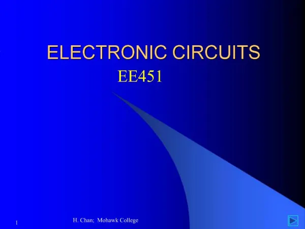
ELECTRONIC CIRCUITS EE451 H. Chan; Mohawk College
MAIN TOPICS (2nd half) • Analog & Switching Power Supplies • Review of rectification & filtering • Review of zener diode as a voltage regulator • Transistor series shunt voltage regulators • Transistor current regulators • IC voltage regulators (e.g. 78/79XX, LM317) • Switching-mode regulators (e.g. LH1605) • Linear Integrated Circuit Applications • BiFET & Norton op-amps, 555 timer, 8038 function generator, active filters, etc. H. Chan; Mohawk College
Power Supply Block Diagram H. Chan; Mohawk College
Half-Wave Rectifier V t H. Chan; Mohawk College
Full-Wave Rectifier V t H. Chan; Mohawk College
Bridge-Type Rectifier V t H. Chan; Mohawk College
More Equations . . . Rearranging the previous equations: VP = Vdc + 1.736 Vr The ripple voltage as a percentage of the dc voltage is: The diode(s) must be rated to withstand the surge current: where RW is the transformer winding’s resistance given by: H. Chan; Mohawk College
Comparison of Different Types of Rectifiers • Half-wave rectifier needs only a single diode but ripple is twice those of the other types. • Full-wave rectifier requires a centre-tapped transformer and its output voltage is about half those of the other types. • Bridge-type rectifier is best overall even though it requires four diodes because the diode bridge is often available in a single package. However, if a single diode in the bridge is defective, the whole package has to be replaced. H. Chan; Mohawk College
Line Regulation is a measure of the effectiveness of a voltage regulator to maintain the output dc voltage constant despite changes in the supply voltage. H. Chan; Mohawk College
Load Regulation is a measure of the ability of a regulator to maintain a constant dc output despite changes in the load current. H. Chan; Mohawk College
Other Specifications A common definition for voltage regulation is: The ability to reduce the output ripple voltage is: Source resistance of regulator is: H. Chan; Mohawk College
Zener Diode Voltage Regulator I-V Characteristic Circuit IZM H. Chan; Mohawk College
Notes on Zener Diode Regulator • VZ depends on I and temperature. • Zener diodes with rated voltage < 6 V have negative temperature coefficient; those rated > 6 V have positive temperature coefficient. • In order to maintain a constant Vo, IZT varies in response to a change of either IL or Vi. For example, when RL increases, IL decreases, then IZT has to increase to keep the current through Rs constant. Since the voltage drop across Rs is constant, Vo stays constant. H. Chan; Mohawk College
Formulae for Zener Regulator Circuit Rs establishes the zener bias current, IZT: For fixed Vi, but variable RL: H. Chan; Mohawk College
Formulae (cont’d) For fixed RL, but variable Vi: The output ripple voltage of the zener regulator is: where RZ = ac resistance of zener diode. H. Chan; Mohawk College
Transistor Series Voltage Regulator The simple zener regulator can be markedly improved by adding a transistor. Since VBE = VZ - VL any tendency for VL to decrease or increase will be negated by an increase or decrease in IE. The dc currents for the circuit are: IL = hFEIB; IZT = IR - IB H. Chan; Mohawk College
Transistor Shunt Voltage Regulator Since VBE = VL - VZ, any tendency for VL to increase or decrease will result in a corresponding increase or decrease in IRs. This will oppose any changes in VL because VL = Vi - IRsRs. IE = IRs - IL = hFEIZT H. Chan; Mohawk College
Op-Amp Voltage Regulators Shunt Series H. Chan; Mohawk College
Notes on Op-Amp Voltage Regulator • More flexibility possible in design of voltage output than IC voltage regulator packages. • The essential circuit elements are: a zener reference, a pass or shunt transistor, a sensing circuit, and an error/amplifier circuit. • Equation indicates that Vo depends on R2, R3, and VZ. • The shunt configuration is less efficient but R2 offers short-circuit current limiting. H. Chan; Mohawk College
Constant Current Limiting can be used for short-circuit or overload protection of the series voltage regulator. Output current is limited to: H. Chan; Mohawk College
Fold-back Current Limiting is a better method of short-circuit protection. H. Chan; Mohawk College
Design Equations for Fold-back Current Limiting Maximum load current without fold-back limiting: Output voltage under current limiting condition: The short circuit current (i.e. when Vo = 0) is: H. Chan; Mohawk College
Characteristics of Fold-back Limiting Vo • Notice that Ishort < IL(max) and that Vo is regulated (i.e. constant) only after RL > a certain critical value. • For designing purpose, R5 + R6 = 1 kW and if Ishort and IL(max) are specified then IL H. Chan; Mohawk College
Transistor Current Regulators are designed to maintain a fixed current through a load for variations in either Vi or RL. For the BJT circuit, VEB = VZ - VRE. Any tendency for IL to change will cause an opposing change in VEB, thus nullifying the perturbation. For the JFET circuit, IL = ID = IDSS as long as VL < VSS - VP. H. Chan; Mohawk College
IC Voltage Regulators • There are basically two kinds of IC voltage regulators: • Multipin type, e.g. LM723C • 3-pin type, e.g. 78/79XX • Multipin regulators are less popular but they provide the greatest flexibility and produce the highest quality voltage regulation • 3-pin types make regulator circuit design simple H. Chan; Mohawk College
Multipin IC Voltage Regulator • The LM723 has an equivalent circuit that contains most of the parts of the op-amp voltage regulator discussed earlier. • It has an internal voltage reference, error amplifier, pass transistor, and current limiter all in one IC package. LM 723C Schematic H. Chan; Mohawk College
Notes on LM723 Voltage Regulator • Can be either 14-pin DIP or 10-pin TO-100 can • May be used for either +ve or -ve, variable or fixed regulated voltage output • Using the internal reference (7.15 V), it can operate as a high-voltage regulator with output from 7.15 V to about 37 V, or as a low-voltage regulator from 2 V to 7.15 V • Max. output current with heat sink is 150 mA • Dropout voltage is 3 V (i.e. VCC > Vo(max) + 3) H. Chan; Mohawk College
LM723 in High-Voltage Configuration Design equations: Choose R1 + R2 = 10 kW, and Cc = 100 pF. External pass transistor and current sensing added. To make Vo variable, replace R1 with a pot. H. Chan; Mohawk College
LM723 in Low-Voltage Configuration With external pass transistor and foldback current limiting Under foldback condition: H. Chan; Mohawk College
Three-Terminal Fixed Voltage Regulators • Less flexible, but simple to use • Come in standard TO-3 (20 W) or TO-220 (15 W) transistor packages • 78/79XX series regulators are commonly available with 5, 6, 8, 12, 15, 18, or 24 V output • Max. output current with heat sink is 1 A • Built-in thermal shutdown protection • 3-V dropout voltage; max. input of 37 V • Regulators with lower dropout, higher in/output, and better regulation are available. H. Chan; Mohawk College
Basic Circuits With 78/79XX Regulators • Both the 78XX and 79XX regulators can be used to provide +ve or -ve output voltages • C1 and C2 are generally optional. C1 is used to cancel any inductance present, and C2 improves the transient response. If used, they should preferably be either 1 mF tantalum type or 0.1 mF mica type capacitors. H. Chan; Mohawk College
Dual-Polarity Output with 78/79XX Regulators H. Chan; Mohawk College
78XX Regulator with Pass Transistor • Q1 starts to conduct when VR2 = 0.7 V. • R2 is typically chosen so that max. IR2 is 0.1 A. • Power dissipation of Q1 is P = (Vi - Vo)IL. • Q2 is for current limiting protection. It conducts when VR1 = 0.7 V. • Q2 must be able to pass max. 1 A; but note that max. VCE2 is only 1.4 V. H. Chan; Mohawk College
78XX Floating Regulator • It is used to obtain an output > the Vreg value up to a max.of 37 V. • R1 is chosen so that R1 0.1 Vreg/IQ, where IQ is the quiescent current of the regulator. or H. Chan; Mohawk College
3-Terminal Variable Regulator • The floating regulator could be made into a variable regulator by replacing R2 with a pot. However, there are several disadvantages: • Minimum output voltage is Vreg instead of 0 V. • IQ is relatively large and varies from chip to chip. • Power dissipation in R2 can in some cases be quite large resulting in bulky and expensive equipment. • A variety of 3-terminal variable regulators are available, e.g. LM317 (for +ve output) or LM 337 (for -ve output). H. Chan; Mohawk College
Basic LM317 Variable Regulator Circuits (a) (b) Circuit with capacitors to improve performance Circuit with protective diodes H. Chan; Mohawk College
Notes on Basic LM317 Circuits • The function of C1 and C2 is similar to those used in the 78/79XX fixed regulators. • C3 is used to improve ripple rejection. • Protective diodes in circuit (b) are required for high-current/high-voltage applications. where Vref = 1.25 V, and Iadj is the current flowing into the adj. terminal (typically 50 mA). R1 = Vref /IL(min), where IL(min) is typically 10 mA. H. Chan; Mohawk College
Other LM317 Regulator Circuits Circuit with pass transistor and current limiting Circuit to give 0V min. output voltage H. Chan; Mohawk College
Block Diagram of Switch-Mode Regulator It converts an unregulated dc input to a regulated dc output. Switching regulators are often referred to as dc to dc converters. H. Chan; Mohawk College
Comparing Switch-Mode to Linear Regulators Advantages: • 70-90% efficiency (about double that of linear ones) • can make output voltage > input voltage, if desired • can invert the input voltage • considerable weight and size reductions, especially at high output power Disadvantages: • More complex circuitry • Potential EMI problems unless good shielding, low-loss ferrite cores and chokes are used H. Chan; Mohawk College
General Notes on Switch-Mode Regulator The duty cycle of the series transistor (power switch) determines the average dc output of the regulator. A circuit to control the duty cycle is the pulse-width modulatorshown below: H. Chan; Mohawk College
General Notes cont’d . . . • The error amplifier compares a sample of the regulator Vo to an internal Vref. The difference or error voltage is amplified and applied to amodulator where it is compared to a triangle waveform. The result is an output pulse whose width is proportional to the error voltage. • Darlington transistors and TMOS FETs with fT of at least 4 MHz are often used. TMOS FETs are more efficient. • A fast-recovery rectifier, or a Schottky barrier diode (sometimes referred to as a catch diode) is used to direct current into the inductor. • For proper switch-mode operation, current must always be present in the inductor. H. Chan; Mohawk College
Step-Down or Buck Converter • When the transistor is turned ON, VL is initially high but falls exponentially while IL increases to charge C. • When the transistor turns OFF, VL reverses in polarity to maintain the direction of current flow. IL decreases but its path is now through the forward-biased diode, D. • Duty cycle is adjusted according to the level of Vo. H. Chan; Mohawk College
V & I Waveforms for Buck Regulator PWM output VL IL Vo Normal Low Vo High Vo H. Chan; Mohawk College
Equations for Buck Regulator Selecting IL = 0.4Io where Io is the max. dc output current: where V is the ripple voltage H. Chan; Mohawk College
Notes on Operation of Buck Regulator • When IL = 0.4Io was selected, the average minimum current, Imin, that must be maintained in L for proper regulator operation is 0.2Io. • If IL is chosen to be 4% instead of 40% of Io, the 2.5 factor in the equation for L becomes 25 and Imin becomes 0.02Io. • L and C are both proportional to 1/fosc; hence, the higher fosc is the smaller L and C become. But for predictable operation and less audible noise, fosc is usually between 50kHz to 100 kHz. H. Chan; Mohawk College
Step-Up, Flyback, or Boost Regulator • Assuming steady-state conditions, when the transistor is turned ON, L reacts against Vin. D is reverse-biased and C supplies the load current. • When the transistor is OFF, VL reverses polarity causing current to flow through D and charges C. Note that Vout is > Vin because VL adds on to Vin. H. Chan; Mohawk College
Equations for Boost Regulator Assuming IL = 0.4Io: H. Chan; Mohawk College
Voltage-Inverting or Buck-Boost Regulator • Vo can be either step-up or step-down and its polarity is opposite to input. • During ON period, Vin is across L, and D is reverse-biased. • During OFF period, VL reverses polarity causing current to flow through C and D. H. Chan; Mohawk College
Equations for Buck-Boost Regulator For IL = 0.4Io: H. Chan; Mohawk College