FRL Transmitter Mezzanine: Configurations & Backplane IO
110 likes | 134 Vues
Explore the FRL Transmitter Mezzanine with 8 configurations and backplane IO options. Test setups and conclusions from the study by Dominique Gigi at CMSweek 6 June 2003.

FRL Transmitter Mezzanine: Configurations & Backplane IO
E N D
Presentation Transcript
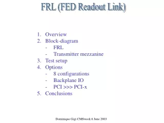
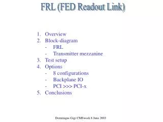
FRL (FED Readout Link) • Overview • Block-diagram • FRL • Transmitter mezzanine • Test setup • Options • 8 configurations • Backplane IO • PCI >>> PCI-x • Conclusions Dominique Gigi CMSweek 6 June 2003
Overview Dominique Gigi CMSweek 6 June 2003
Block Diagram 64b @ 66 or 100MHz Commercial Optical Link Myrinet Lanai X 64kB IN_1 PCI connector 64-bit 64kB PCI 64b @ 66 or PCI-x 64b @ 100MHz FRL Function IN_2 FPGA 64kB Bridge IN_3 FPGA Memory 4Mbytes Compact PCI Back-plane 64b@100MHz Compact PCI 32-bit 33MHz 64kB IN_4 Dominique Gigi CMSweek 6 June 2003
Transmitter Mezzanine SLink64 protocol LVDS Altera ACEX LVDS • Generate 3 frequencies: • 40MHz from 10 to 15 meters • 60MHz from 5 to 10 meters • 80MHz <= 5 meters 1 switch to choose the frequency Dominique Gigi CMSweek 6 June 2003
Test setup Myrinet protocol emulator Acquisition (64b-66MHz) LVDS 640MB/s FRL Spy mode (Event_ID# 1 to 1024) FED emulator PCI to CompactPCI PC Dominique Gigi CMSweek 6 June 2003
Test setup (data flow) Event_ID Event_size (bytes) BX_id Source# Time (x100ns) before next event FED_emu1 (GIII) FRL PCI 64b@66MHz Myr_protocol_emu (GIII) H FRL_Myrinet protocol T H H T Event(t) Event(t+1) Event(t-1) WAIT WAIT H T 64kB LVDS Packet size Source# Event_ID H H Packet# FED2 FED1 FRL FPGA reserved Pack. size FED_emu2 (GIII) reserved Spy mode 64kB From 1 to 2 M event descriptors Using SDRAM memory Host_PC Bridge LVDS PC memory ZBT memory Data block size T H FED-kit Event(t) Event(t+1) Event(t-1) WAIT WAIT Block0 H T H Block1 Block2 Block3 Block4 PCI to CPCI link T Block5 Block6 Block7 Block8 Block9 Blockn WC_E0 WC_E1 Dominique Gigi CMSweek 6 June 2003
FPGA Configuration Flash memory Add[2..0] FRL diagnostic 111 FRL (Evt generator) 110 101 FRL (Evt memory) Bus to FPGA configuration 100 011 010 001 000 (configuration by default POWER ON) FRL with Input Accessed through PCI Bridge configuration Signal to reconfigure FPGA 128 ms to load a design from Flash to FPGA NB: Bridge design (EEPROM) and FRL (FLASH) designs can be downloaded through the PCI Bridge configuration. Dominique Gigi CMSweek 6 June 2003
IO's backplane It’s not a bus each FRL has its individual pins Lemo • 16 IO’s FRL • 15 IO’s Bridge • 5 v • 3.3v • -12v • +12v • GND Ethernet Compact PCI backplane CompactPCI bus 32-bit@33MHz Dominique Gigi CMSweek 6 June 2003
AD[63..0] FRAME IRDY TRDY Addr Data AD[63..0] FRAME IRDY TRDY Addr Attr Data PCI (66MHz) ---- PCI-x (100MHz) -Access to the LanaiX configuration -Pending data transfer PCI-x bus 64-bit 100 MHz Bridge Convert PCI access (32-bit@33MHz) to PCI-x access (64-bit@100MHz) Dominique Gigi CMSweek 6 June 2003
Setup to test production • 4 points to control: • Inputs (Connectors, FIFO,LVDS,FPGA) • PCI bus • ZBT memory (data, address, control) • JTAG • One PC controls 16 FRLs (CompactPCI backplane) • GIII generates events and receives them through PCI to control data and header registers report errors • ZBT is tested through the SPY mode application • JTAG is tested with JAM-Player (adapted by Christoph) access the JTAG chain through PCI bus Dominique Gigi CMSweek 6 June 2003
Conclusions • PCI-x protocol is tested (without data transfer; single access) • The 2 Inputs were debugged • ZBT memory access (64b@100MHz) • Start the setup implementation for test production • Pending • transfer data with PCI-x protocol to Myrinet LanaiX • merge function (logic – no hardware) • CRC implementation (FED_emu + check inside FRL) Dominique Gigi CMSweek 6 June 2003


![[EPUB] DOWNLOAD Classic Battletech: Technical Readout: Vehicle Annex (FPR35022)](https://cdn7.slideserve.com/12426293/slide1-dt.jpg)