Programmable Logic Arrays: CS 150 Spring 2007
Delve into the study of Programmable Logic Arrays in CS 150 Spring 2007 lecture series. Explore topics like PLAs, terms, connections, and efficient design techniques.

Programmable Logic Arrays: CS 150 Spring 2007
E N D
Presentation Transcript
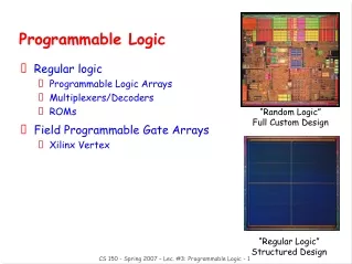
Programmable Logic • Regular logic • Programmable Logic Arrays • Multiplexers/Decoders • ROMs • Field Programmable Gate Arrays • Xilinx Vertex “Random Logic” Full Custom Design “Regular Logic” Structured Design CS 150 - Spring 2007 – Lec. #3: Programmable Logic - 1
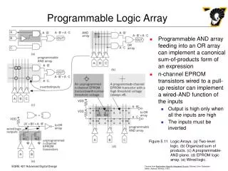
• • • inputs ORarray ANDarray productterms outputs • • • Programmable Logic Arrays (PLAs) • Pre-fabricated building block of many AND/OR gates • Actually NOR or NAND • ”Personalized" by making or breaking connections among gates • Programmable array block diagram for sum of products form CS 150 - Spring 2007 – Lec. #3: Programmable Logic - 2
product inputs outputs term A B C F0 F1 F2 F3AB 1 1 – 0 1 1 0B'C – 0 1 0 0 0 1AC' 1 – 0 0 1 0 0B'C' – 0 0 1 0 1 0A 1 – – 1 0 0 1 reuse of terms Enabling Concept • Shared product terms among outputs F0 = A + B' C' F1 = A C' + A B F2 = B' C' + A B F3 = B' C + A example: input side: personality matrix 1 = uncomplemented in term 0 = complemented in term – = does not participate output side: 1 = term connected to output 0 = no connection to output CS 150 - Spring 2007 – Lec. #3: Programmable Logic - 3
Before Programming • All possible connections available before "programming" • In reality, all AND and OR gates are NANDs CS 150 - Spring 2007 – Lec. #3: Programmable Logic - 4
B C A AB B'C AC' B'C' A F0 F1 F2 F3 After Programming • Unwanted connections are "blown" • Fuse (normally connected, break unwanted ones) • Anti-fuse (normally disconnected, make wanted connections) CS 150 - Spring 2007 – Lec. #3: Programmable Logic - 5
A B C D AB A'B' CD' C'D AB+A'B' CD'+C'D Alternate Representation for High Fan-in Structures • Short-hand notation--don't have to draw all the wires • Signifies a connection is present and perpendicular signal is an input to gate notation for implementing F0 = A B + A' B' F1 = C D' + C' D CS 150 - Spring 2007 – Lec. #3: Programmable Logic - 6
A B C A'B'C' A'B'C A'BC' A'BC AB'C' AB'C ABC' ABC A B C F1 F2 F3 F4 F5 F6 0 0 0 0 0 1 1 0 0 0 0 1 0 1 0 1 1 1 0 1 0 0 1 0 1 1 1 0 1 1 0 1 0 1 0 0 1 0 0 0 1 0 1 1 1 1 0 1 0 1 0 1 0 0 1 1 0 0 1 0 1 0 0 1 1 1 1 1 0 0 1 1 F1 F2 F3 F4 F5 F6 Programmable Logic Array Example • Multiple functions of A, B, C • F1 = A B C • F2 = A + B + C • F3 = A' B' C' • F4 = A' + B' + C' • F5 = A xor B xor C • F6 = (A xnor B xnor C)’ full decoder as for memory address bits stored in memory CS 150 - Spring 2007 – Lec. #3: Programmable Logic - 7
A A A A 0 0 X 1 1 0 X 0 0 1 X X 1 0 X X 0 1 X 0 0 1 X 0 0 0 X X 0 0 X X 0 0 X 1 0 1 X 1 0 1 X X 0 1 X X 0 1 X 0 0 1 X 0 1 1 X X 1 1 X X D D D D C C C C A B C D W X Y Z0 0 0 0 0 0 0 00 0 0 1 0 0 0 10 0 1 0 0 0 1 10 0 1 1 0 0 1 00 1 0 0 0 1 1 00 1 0 1 1 1 1 00 1 1 0 1 0 1 00 1 1 1 1 0 1 11 0 0 0 1 0 0 11 0 0 1 1 0 0 01 0 1 – – – – –1 1 – – – – – – B B B B PLA Design Example • BCD to Gray code converter K-map for W K-map for X minimized functions: W = A + B D + B C X = B C' Y = B + C Z = A'B'C'D + B C D + A D' + B' C D' K-map for Y K-map for Z CS 150 - Spring 2007 – Lec. #3: Programmable Logic - 8
A B C D A BD BC BC' B C A'B'C'D BCD AD' BCD' W X Y Z PLA Design Example (cont’d) • Code converter: programmed PLA minimized functions: W = A + B D + B C X = B C' Y = B + C Z = A'B'C'D + B C D + A D' + B' C D' not a particularly good candidate for PLA implementation since no terms are shared among outputs however, much more compact and regular implementation when compared with discrete AND and OR gates CS 150 - Spring 2007 – Lec. #3: Programmable Logic - 9
A B C D W X Y Z0 0 0 0 0 0 0 00 0 0 1 0 0 0 10 0 1 0 0 0 1 10 0 1 1 0 0 1 00 1 0 0 0 1 1 00 1 0 1 1 1 1 00 1 1 0 1 0 1 00 1 1 1 1 0 1 11 0 0 0 1 0 0 11 0 0 1 1 0 0 01 0 1 – – – – –1 1 – – – – – –A B C D W X Y Z0 0 0 0 0 0 0 00 0 0 1 0 0 0 10 0 1 0 0 0 1 10 0 1 1 0 0 1 00 1 0 0 0 1 1 00 1 0 1 1 1 1 00 1 1 0 1 0 1 00 1 1 1 1 0 1 11 0 0 0 1 0 0 11 0 0 1 1 0 0 01 0 1 – – – – –1 1 – – – – – – PLA Design Example • BCD to Gray code converter A A 0 0 X 1 0 1 X 1 0 1 X X 0 1 X X 0 1 X 0 0 1 X 0 0 0 X X 0 0 X X D D C C B B K-map for W K-map for X A A 0 1 X 0 0 1 X 0 1 1 X X 1 1 X X 0 0 X 1 1 0 X 0 0 1 X X 1 0 X X minimized functions: W = X = Y = Z = D D C C B B K-map for Y K-map for Z CS 150 - Spring 2007 – Lec. #3: Programmable Logic - 10
A B C D W X Y Z0 0 0 0 0 0 0 00 0 0 1 0 0 0 10 0 1 0 0 0 1 10 0 1 1 0 0 1 00 1 0 0 0 1 1 00 1 0 1 1 1 1 00 1 1 0 1 0 1 00 1 1 1 1 0 1 11 0 0 0 1 0 0 11 0 0 1 1 0 0 01 0 1 – – – – –1 1 – – – – – –A B C D W X Y Z0 0 0 0 0 0 0 00 0 0 1 0 0 0 10 0 1 0 0 0 1 10 0 1 1 0 0 1 00 1 0 0 0 1 1 00 1 0 1 1 1 1 00 1 1 0 1 0 1 00 1 1 1 1 0 1 11 0 0 0 1 0 0 11 0 0 1 1 0 0 01 0 1 – – – – –1 1 – – – – – – PLA Design Example #1 • BCD to Gray code converter A A 0 0 X 1 0 1 X 1 0 1 X X 0 1 X X 0 1 X 0 0 1 X 0 0 0 X X 0 0 X X D D C C B B K-map for W K-map for X BC’ A A 0 1 X 0 0 1 X 0 1 1 X X 1 1 X X 0 0 X 1 1 0 X 0 0 1 X X 1 0 X X minimized functions: W = X = Y = Z = D D C C B B K-map for Y K-map for Z CS 150 - Spring 2007 – Lec. #3: Programmable Logic - 11
Multiplexer/Demultiplexer: Making Connections • Direct point-to-point connections between gates • Multiplexer: route one of many inputs to a single output • Demultiplexer: route single input to one of many outputs control control multiplexer demultiplexer 4x4 switch CS 150 - Spring 2007 – Lec. #3: Programmable Logic - 13
I1 I0 A Z0 0 0 00 0 1 00 1 0 10 1 1 01 0 0 01 0 1 11 1 0 11 1 1 1I1 I0 A Z0 0 0 00 0 1 00 1 0 10 1 1 01 0 0 01 0 1 11 1 0 11 1 1 1 A Z0 I01 I1 Multiplexers/Selectors • Multiplexers/Selectors: general concept • 2n data inputs, n control inputs (called "selects"), 1 output • Used to connect 2n points to a single point • Control signal pattern forms binary index of input connected to output Z = A' I0 + A I1 functional form logical form two alternative forms for a 2:1 Mux truth table CS 150 - Spring 2007 – Lec. #3: Programmable Logic - 14
I0I1I2I3I4I5I6I7 8:1mux Z I0I1I2I3 4:1mux Z I0I1 2:1mux Z A A B A B C Multiplexers/Selectors (cont'd) • 2:1 mux: Z = A' I0 + A I1 • 4:1 mux: Z = A' B' I0 + A' B I1 + A B' I2 + A B I3 • 8:1 mux: Z = A'B'C'I0 + A'B'CI1 + A'BC'I2 + A'BCI3 + AB'C'I4 + AB'CI5 + ABC'I6 + ABCI7 • In general, Z = (mkIk) • in minterm shorthand form for a 2n:1 Mux n 2 -1 k=0 CS 150 - Spring 2007 – Lec. #3: Programmable Logic - 15
I0I1I2I3 8:1mux 4:1mux Z 2:1mux I4I5I6I7 I0I1 8:1mux 2:1mux 4:1mux I2I3 2:1mux 4:1mux Z B C A I4I5 2:1mux I6I7 2:1mux A B C Cascading Multiplexers • Large multiplexers implemented by cascading smaller ones alternativeimplementation control signals B and C simultaneously choose one of I0, I1, I2, I3 and one of I4, I5, I6, I7control signal A chooses which of theupper or lower mux's output to gate to Z CS 150 - Spring 2007 – Lec. #3: Programmable Logic - 16
10100011 01234567 F 8:1 MUX S2 S1 S0 A B C Multiplexers as Lookup Tables (LUTs) • 2n:1 multiplexer implements any function of n variables • With the variables used as control inputs and • Data inputs tied to 0 or 1 • In essence, a lookup table • Example: • F(A,B,C) = m0 + m2 + m6 + m7 = A'B'C' + A'BC' + ABC' + ABC = A'B'(C') + A'B(C') + AB'(0) + AB(1) CS 150 - Spring 2007 – Lec. #3: Programmable Logic - 17
10100011 01234567 A B C F0 0 0 10 0 1 00 1 0 10 1 1 01 0 0 01 0 1 01 1 0 11 1 1 1 C'C'01 C'C'01 0123 F 4:1 MUX 8:1 MUX S1 S0 A B S2 S1 S0 A B C Multiplexers as LUTs (cont’d) • 2n-1:1 mux can implement any function of n variables • With n-1 variables used as control inputs and • Data inputs tied to the last variable or its complement • Example: • F(A,B,C) = m0 + m2 + m6 + m7 = A'B'C' + A'BC' + ABC' + ABC = A'B'(C') + A'B(C') + AB'(0) + AB(1) F CS 150 - Spring 2007 – Lec. #3: Programmable Logic - 18
1D01D’DD’D’ 01234567 A 1 1 0 0 1 0 1 0 8:1 MUX D 0 1 1 0 1 1 0 1 S2 S1 S0 C B A B C Multiplexers as LUTs (cont’d) • Generalization • Example: F(A,B,C,D) implemented by an 8:1 MUX I0 I1 . . . In-1 In F. . . . 0 0 011. . . . 1 0 101 0 In In' 1 four possible configurationsof truth table rows can be expressedas a function of In • n-1 mux control variables • single mux data variable choose A,B,C as control variablesmultiplexer implementation CS 150 - Spring 2007 – Lec. #3: Programmable Logic - 19
Announcements • We took everyone on the wait list into the class • Result is that evening labs are very crowded! • Think of switching to mid-day labs to get more TA face time! • First three labs are done individually … need not commit to a project partner yet • Send email to jeff@sims.berkeley.edu to request a lab change • First HW due Friday at 2 PM … just before Lab Lecture • CS 150 hand-in box outside and just to the right of 125 Cory doors • Discussions Th@4, F@10, 11 to work through old homeworks in 125 Cory • Second HW soon on class web site • Use google ucb.class.cs150 newsgroup for lab, hw, course questions! CS 150 - Spring 2007 – Lec. #3: Programmable Logic - 20
1 1 1 1 Read-only Memories • Two dimensional array of 1s and 0s • Entry (row) is called a "word" • Width of row = word-size • Index is called an "address" • Address is input • Selected word is output word lines (only one is active – decoder is just right for this) n 2 -1 i word[i] = 0011word[j] = 1010 decoder j 0 internal organization • 0 n-1 • Address bit lines (normally pulled to 1 through resistor – selectively connected to 0 by word line controlled switches) CS 150 - Spring 2007 – Lec. #3: Programmable Logic - 25
A B C F0 F1 F2 F3 0 0 0 0 0 1 00 0 1 1 1 1 00 1 0 0 1 0 00 1 1 0 0 0 1 1 0 0 1 0 1 1 1 0 1 1 0 0 0 1 1 0 0 0 0 1 1 1 1 0 1 0 0 ROM8 words x 4 bits/word A B C F0 F1 F2 F3 address outputs truth table block diagram ROMs and Combinational Logic • Combinational logic implementation (two-level canonical form) using a ROM F0 = A' B' C + A B' C' + A B' C F1 = A' B' C + A' B C' + A B C F2 = A' B' C' + A' B' C + A B' C' F3 = A' B C + A B' C' + A B C' CS 150 - Spring 2007 – Lec. #3: Programmable Logic - 26
n address lines • • • inputs memoryarray(2n wordsby m bits) decoder 2n wordlines outputs • • • m data lines ROM Structure • Similar to a PLA structure but with a fully decoded AND array • Completely flexible OR array (unlike PAL) CS 150 - Spring 2007 – Lec. #3: Programmable Logic - 27
Field-Programmable Gate Arrays • PLAs: 100s of gate equivalents • FPGAs: 1000-10000s gates • Logic blocks • Implement combinationaland sequential logic • Interconnect • Wires to connect inputs andoutputs to logic blocks • I/O blocks • Special logic blocks at periphery of device forexternal connections • Key questions: • How to make logic blocks programmable? • How to connect the wires? • After the chip has been fabbed CS 150 - Spring 2007 – Lec. #3: Programmable Logic - 29
Tradeoffs in FPGAs • Logic block - how are functions implemented: fixed functions (manipulate inputs) or programmable? • Support complex functions, need fewer blocks, but they are bigger so less of them on chip • Support simple functions, need more blocks, but they are smaller so more of them on chip • Interconnect • How are logic blocks arranged? • How many wires will be needed between them? • Are wires evenly distributed across chip? • Programmability slows wires down – are some wires specialized to long distances? • How many inputs/outputs must be routed to/from each logic block? • What utilization are we willing to accept? 50%? 20%? 90%? CS 150 - Spring 2007 – Lec. #3: Programmable Logic - 30
Xilinx 4000 Series Programmable Gate Arrays • CLB - Configurable Logic Block • 5-input, 1 output function • or 2 4-input, 1 output functions • optional register on outputs • Built-in fast carry logic • Can be used as memory • Three types of routing • direct • general-purpose • long lines of various lengths • RAM-programmable • can be reconfigured CS 150 - Spring 2007 – Lec. #3: Programmable Logic - 31
The Xilinx 4000 CLB CS 150 - Spring 2007 – Lec. #3: Programmable Logic - 32
Two 4-Input Functions, Registered Output CS 150 - Spring 2007 – Lec. #3: Programmable Logic - 33
5-Input Function, Combinational Output CS 150 - Spring 2007 – Lec. #3: Programmable Logic - 34
CLB Used as RAM CS 150 - Spring 2007 – Lec. #3: Programmable Logic - 35
Xilinx 4000 Interconnect CS 150 - Spring 2007 – Lec. #3: Programmable Logic - 36
Xilinx FPGA Combinational Logic Examples • Key: General functions are limited to 5 inputs • (4 even better - 1/2 CLB) • No limitation on function complexity • Example • 2-bit comparator: A B = C D and A B > C D implemented with 1 CLB(GT) F = A C' + A B D' + B C' D' (EQ) G = A'B'C'D'+ A'B C'D + A B'C D'+ A B C D • Can implement some functions of > 5 input CS 150 - Spring 2007 – Lec. #3: Programmable Logic - 37
Xilinx FPGA Combinational Logic • Examples • N-input majority function: 1 whenever n/2 or more inputs are 1 • N-input parity functions: 5 input/1 CLB; 2 levels yield 25 inputs! 5-input Majority Circuit 9 Input Parity Logic CLB CLB 7-input Majority Circuit CLB CLB CLB CLB CS 150 - Spring 2007 – Lec. #3: Programmable Logic - 38
Xilinx FPGA Adder Example • Example • 2-bit binary adder - inputs: A1, A0, B1, B0, CIN outputs: S0, S1, Cout Full Adder, 4 CLB delays to final carry out 2 x Two-bit Adders (3 CLBs each) yields 2 CLBs to final carry out CS 150 - Spring 2007 – Lec. #3: Programmable Logic - 39
Combinational Logic Implementation Summary • Regular Logic Structures • Programmable Logic Arrays • Programmable connections: AND-OR (NOR-NOR) Arrays • Multiplexers/decoders • Multipoint connections for signal routing • Lookup Tables • ROMs • Truth table in hardware • Field Programmable Gate Arrays (FPGAs) • Programmable logic (LUTs, Truth Tables) and connections • Advantages/disadvantages of each CS 150 - Spring 2007 – Lec. #3: Programmable Logic - 40