Design and Implementation of Programmable Logic Arrays (PLAs)
Explore how to program, customize, and utilize PLAs efficiently in logic circuit design, including PALs, ROMs, and more.


Design and Implementation of Programmable Logic Arrays (PLAs)
E N D
Presentation Transcript
Programmable Logic PAL, PLA
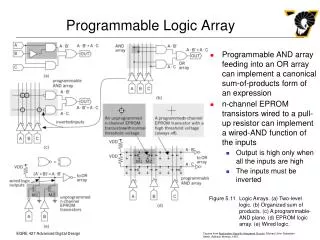
PLAs Programmable Logic Array • Pre-fabricated building block of many AND/OR gates (or NOR, NAND) "Personalized" by making/ breaking connections among the gates. • General purpose logic building blocks.
PLA • A 3×2 PLA with 4 product terms.
Product Inputs Outputs t erm F F F F A B C 0 1 2 3 0 1 1 0 A B 1 1 - Reuse 0 0 0 1 B C - 0 1 of 0 1 0 0 A C 1 - 0 t erms 1 0 1 0 B C - 0 0 1 0 0 1 A 1 - - Design for PLA:Example • Implement the following functions using PLA F0 = A + B' C' F1 = A C' + A B F2 = B' C' + A B F3 = B' C + A Input Side: 1 = asserted in term 0 = negated in term - = does not participate Personality Matrix Output Side: 1 = term connected to output 0 = no connection to output
A C B AB B’C AC’ B’C’ A F1 F0 F3 F2 Example: Continued F0 = A + B' C' F1 = A C' + A B F2 = B' C' + A B F3 = B' C + A Personality Matrix
Constants • Sometimes a PLA output must be programmed to be a constant 1 or a constant 0. • P1 is always 1 because its product line is connected to no inputs and is therefore always pulled HIGH; • this constant-1 term drives the O1 output. • No product term drives the O2 output, which is therefore always 0. • Another method of obtaining a constant-0 output is shown for O3.
BCD to Gray Code Converter Minimized Functions: W = A + B D + B C X = B C' Y = B + C Z = A'B'C'D + B C D + A D' + B' C D'
A B C D A BD 4 product terms per each OR gate BC BC’ Product terms cannot be shared ! B PLA achieves higher flexibility at the cost of lower speed! C BCD AD’ BCD’ W X Y Z
PALs • Programmable Array Logic • a fixed OR array.
PAL inputs 1st output section Only functions with at most four products can be implemented 2nd output section 3rd output section 4th output section
PAL x x x W = ABC + CD X = ABC + ACD + ACD + BCD Y = ACD + ACD + ABD
Helper Terms • If an I/O pin’s output-control gate produces a constant 1, the output is always enabled, but the pin may still be used as an input too. • outputs can be used to generate first-pass “helper terms” for logic functions that cannot be performed in a single pass with the limited number of AND terms available for a single output.
Read-Only Memory ROM
0 A ‘B’C’D’ 1 A ‘B’C’D F 1 2 A ‘B’CD’ 3 A ‘B’CD S3 A 4 A ‘BC’D’ 5 A ‘BC’D S2 B 6 A ‘BCD’ 4:16 7 A ‘ BCD dec S1 C 8 A B’C’D’ F 2 9 A B’C’D S0 10 A B’CD’ D 1 1 A B’CD 12 A B C’D’ 13 A B C’D 14 A B C D’ F 3 15 A B C D Enb ROM • Decoder • Produces minterms • ORs • Produce SOP’s
X X X D7 D6 X X D5 X D4 D3 A2 A X D2 X X B A1 D1 X A0 D0 C F0 F2 F1 F3 ROM • ROM • A decoder • A set of programmable OR’s
ROM vs. PLA/PAL Fixed Programmable Programmable Inputs Outputs AND array Connections OR array (decoder) (a) Programmable read-only memory (PROM) Programmable Programmable Fixed Inputs Outputs Connections AND array OR array (b) Programmable array logic (PAL) device Programmable Programmable Programmable Programmable Outputs Inputs Connections Connections AND array OR array (c) Programmable logic array (PLA) device
Example • Find a ROM-based circuit implementation for: • f(a,b,c) = a’b’ + abc • g(a,b,c) = a’b’c’ + ab + bc • h(a,b,c) = a’b’ + c • Solution: • Express f(), g(), and h() in m()format (use truth tables) • Program the ROM based on the 3 m()’s
a 0 1 2 3 4 5 6 7 3-to-8decoder b c g f h Example • There are 3 inputs and 3 outputs, thus we need a 8x3 ROM block. • f = m(0, 1, 7) • g = m(0, 3, 6, 7) • h = m(0, 1, 3, 5, 7)
ROM as a Memory • Read Only Memories (ROM) or Programmable Read Only Memories (PROM) have: • N input lines, • M output lines, and • 2N decoded minterms. • Can be viewed as a memory with the inputs as addresses of data (output values), • hence ROM or PROM names!
(Memories) • Volatile: • Random Access Memory (RAM): • SRAM "static" • DRAM "dynamic" • Non-Volatile: • Read Only Memory (ROM): • Mask ROM "mask programmable" • EPROM "electrically programmable" • EEPROM “electrically erasable electrically programmable" • FLASH memory - similar to EEPROM with programmer integrated on chip
X X X D0 D1 X X D2 X D3 D4 A2 A X D5 X X B A1 D6 X A0 D7 C F3 F1 F2 F0 ROM as Memory • Read Example: For input (A2,A1,A0) = 011, output is (F0,F1,F2,F3 ) = 0010. • What are functions F3, F2 , F1 and F0 in terms of (A2, A1, A0)? Address 8x4 ROM A[2:0] F[3:0] 3 4
Design by ROM: Example • BCD to 7 Segment Display Controller C0 C1 C2 C3 C4 C5 C6 A B C D 0 0 0 0 0 0 0 1 0 0 1 0 0 0 1 1 0 1 0 0 0 1 0 1 0 1 1 0 0 1 1 1 1 1 1 1 1 1 0 0 1 1 0 0 0 0 1 1 0 1 1 0 1 1 1 1 1 0 0 1 0 1 1 0 0 1 1 1 0 1 1 0 1 1 1 0 1 1 1 1 1 1 1 1 0 0 0 0 1 1 1 1 1 1 1 1 1 1 0 0 1 1 1 0 0 0 1 0 0 1 1 0 1 0 1 0 1 1 1 1 0 0 1 1 0 1 1 1 1 0 0 1 1 1 X X X X X X X X X X X X X X X X X X X X X X X X X X X X X X X X X X X X X X X X X X
Standard Devices • Vpp and PGM are used when programming 2764 EPROM 8K x 8