Programmable Logic
Programmable Logic. There are other ways to implement a logic function than to hook together discrete 74XX packages or create a custom Integrated Circuit. Memory - can use semiconductor memory to implement logic equations

Programmable Logic
E N D
Presentation Transcript
Programmable Logic • There are other ways to implement a logic function than to hook together discrete 74XX packages or create a custom Integrated Circuit. • Memory - can use semiconductor memory to implement logic equations • Programmable Logic - can use integrated circuits known as “Programmable Logic Devices” to implement logic.
Memory We typically think of a memory device as used for storing data. A Memory chip is characterized by how many locations it contains and how many bits per location it can hold. Memories are classified as K x m devices, K is the # of locations, m is the number bits per location (16 x 2 would be 16 locations, each storing 2 bits). To access a LOCATION within a memory device, a group of inputs known as the ADDRESS BUS is used. The number of address lines needed is n = log2(K) (I.e., for 16 locations would need 4 address lines). The data at a location is placed on some outputs known as the DATA bus.
Memory Examples 32 x 8 memory (32 locations, 8 bits per location). Needs 5 address lines, 8 data lines D[7:0] A[4:0] 32 x 8 5 8 64 x 2 memory (64 locations, 2 bits per location). Needs 6 address lines, 2 data lines D[1:0] A[5:0] 64 x 2 2 6
LookUp Table (LUT) Loc A B C D F(A,B,C,D) 0 0 0 0 0 0 1 0 0 0 1 0 2 0 0 1 0 1 3 0 0 1 1 1 4 0 1 0 0 0 5 0 1 0 1 0 6 0 1 1 0 1 7 0 1 1 1 0 8 1 0 0 0 0 9 1 0 0 1 010 1 0 1 0 111 1 0 1 1 012 1 1 0 0 013 1 1 0 1 114 1 1 1 0 115 1 1 1 1 1 A memory device can be thought of as a LookUp Table (LUT), in which each location contains 1 or more bits. 16 x 1 Memory A A3A2A1A0 O B F C D
ROM Implementation of Boolean Functions Contents of ROM usually specified by a truth table A 2n x m ROM can realize m functions of n variables Decoder generates all minterms of input variables Switching elements effectively form an OR gate e.g. F0 = m0+m1+m4+m6
Example: Code Converter “Dots” represent Switching elements.
A B C F G 0 0 0 0 0 0 0 1 1 0 0 1 0 1 0 0 1 1 0 1 1 0 0 1 0 1 0 1 0 1 1 1 0 0 1 1 1 1 1 1 A B Y0 0 00 1 11 0 11 1 0 Example: Implement 2 functions of 3 variables F (A,B,C) = A B C G = AB + AC + BC 8 x 2 Memory A G A2 O1 B A1 F O0 C A0 LookUp Table (LUT) A[2:0] is 3 bit address bus, O[1:0] is 2 bit output bus.Location 0 has “00”, Location 1 has “10”,Location 2 has “10”, etc…. Recall that Exclusive OR ()
Memory Implementation can be INEFFICIENT What if I wanted to implement: F(A,B,C, D) and G (W,X,Y, Z) These are two INDEPENDENT functions - they use DIFFERENT inputs! Note that the variables are different. I could use two different memory devices (need 32 locations total between the two devices): 16 x 1 Memory 16 x 1 Memory A W A3A2A1A0 O A3A2A1A0 O F G B X C Y D Z
Memory Implementation can be INEFFICIENT (Cont’d) What if I wanted to use only a single memory device? 256 x 2 Memory Went from 32 locations to 256 locations! A A7A6A5A4 O1O0 G B C F D Most of the locations are wasted because I have to repeat the G function for every F input. W A3A2A1A0 X Y Z
Another Inefficiency Implement: F(A,B,C,D,E,F,G,H) = ABCD + EFGH Looks like a simple equation…would only take two 4 input NANDs, and one two input NAND (NAND-NAND form). Yet it takes a 256 x 1 memory device because of the number of input variables! 256 x 1 Memory A A7A6A5A4 O B C F D E A3A2A1A0 F G H
Memory Summary • To implement m functions of the same n variables, need a memory with 2nlocations and m bits per location (use one address line for each variable, use data out line for each function). • Memory is not efficient at implementing wide functions (functions with lots of input variables) or multiple functions with different inputs.
Programmable Logic Devices (PLDs) • PLDs were invented to address the inefficiencies of implementing logic using memories. • PLDs can implement wide functions efficiently (functions with many input variables). • PLDs can implement multiple functions of different variables efficiently. • The logic in PLDs is programmable -- it can be defined by the user and programmed on the desktop • Most PLDs can be erased and reprogrammed many times.
PLD types • There are MANY different types of PLDs. • Densities ranges from from 10’s of gates to 100’s of thousands of gates. • We will look at a type called PALs (Programmable Array Logic).
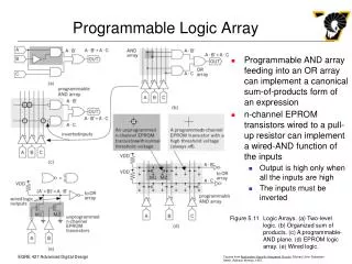
Programmable Logic Array PLA n input lines AND Array OR Array AND array --> product terms OR array OR’s together product terms k word lines m output lines Can realize m functions of n variables
PLA Internal Structure A B C OR Array PLA AND-OR Array Equivalent AND Array F1 F0 F2 F3
PLA Realization of Functions F1 = a’bd + abd+ab’c’ + b’c F2 = c + a’bd F3 = bc + ab’c’ + abd
PALs (Programmable Array Logic) • An early type of programmable logic - still in common use today. • Logic is represented in SOP form (Sum of Products) • The number of PRODUCTs in an SOP form will be limited to a fixed number (usually 4-10 Product terms). • The number of VARIABLEs in each product term is limited by the number of input pins on the PLD (usually a lot, minimum of 10 inputs) • The number of independent functions is limited by number of OUTPUT pins.
A G B H C I D J P E Q R F K A Sample PAL
Comments on Sample PAL • 11 inputs, 3 outputs • Can implement three functions • Each output implements a SOP equation with four product terms. • Each product term can include complemented or uncomplemented form of an input.
Understanding the Diagram D J P Horizontal Lines indicate a product term. Vertical lines provide True and Complemented forms of external inputs. Even though a product term looks like it has only one input, it actually has 2 * N inputs, where N is the number of external inputs.
Product Term B B’A A’ C C’ D D’I I’ J J’ E E’ F F’ K K’GG’H H’ This looks like an AND gate with one input. It is actually: B B’ (Assuming all fuses are intact) A A’ C C’ H H’ Only drawn with a single line to save space.
Fuse Points D J P A cross over of a Vertical input line and a horizontal product term line is a FUSE LOCATION. When the PAL is in its blank or erased state, all FUSES are connected. This means that each product term implements the equation: ( A A’ B B’ C C’……. KK’) which will be ‘0’ This means that the output will be high (NOR gate).
Programming D J P To program, we will want to BLOW most of the fuses (break the vertical/horizontal crossover connection). To indicate a logic function, will use a ‘ X ‘ over a fuse that we want to KEEP INTACT. Will mark Intact fuse location. When a fuse is blown, that product term input acts as a ‘1’ so that the input no longer effects the product term.
P’ = D + J’ D J P When implementing an equation, sometimes we will not want to use all available product terms. Mark unused product terms by placing an X over them -- all fuses in that product term row are assumed intact, however the product term is unused, as indicated by the X’d out AND gate. Note that P’ must be implemented (NOR gate).
Example Product Term AC’H’ B B’A A’ C C’ D D’I I’ J J’ E E’ F F’ K K’GG’H H’ The connections will be: 1 Fuse blown 1 Fuse blown A Fuse intact Fuse blown 1 1 Fuse blown Fuse intact C’ 1 Fuse blown H’ Fuse intact Actually, fuses are not ‘blown’ in eraseable PLDs - the connection is broken in a non-destructive way for eraseable PLDs.
Another Example A G B H C I D J P P’ = A’BGH’ + CD’ + HIJ + BG’H
An Optimization Question The following two equations are the same: P’ = A’B’C’D’ + A’BC’D’ + A’B’CD’ P’ = A’C’D’ + A’B’D’ (minimized form) Does it make a difference which form we implement in the previous PLD? NO Each SOP equation in the PLD has four Product terms allocated. An unused PT cannot be used elsewhere - so makes no difference in terms of the amount of resources used in the PLD!!!
Other PLD types • Other types of programmable logic have much different internal structures from PALs. • You must understand the internal structure of whatever PLD you are using so that you can understand the LIMITATIONS and ADVANTAGES of the particular PLD that you are using. • These advantages/limitations can affect how you implement a particular logic function