Download

1 / 73
740 likes | 886 Vues
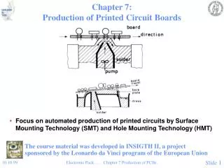
Chapter 7: Production of Printed Circuit Boards. Focus on automated production of printed circuits by Surface Mounting Technology (SMT) and Hole Mounting Technology (HMT). The course material was developed in INSIGTH II, a project sponsored by the Leonardo da Vinci program of the European Union.

E N D
Chapter 7:Production of Printed Circuit Boards • Focus on automated production of printed circuits by Surface Mounting Technology (SMT) and Hole Mounting Technology (HMT) The course material was developed in INSIGTH II, a project sponsored by the Leonardo da Vinci program of the European Union Electronic Pack….. Chapter 7 Production of PCBs.
Hole Mounting • Axial components: Sequencing and mounting • Radial components: Mounting • DIP components: Mounting • Odd components: Robot or hand mounting Fig. 7.1:The process for production of hole mounted PCBs Electronic Pack….. Chapter 7 Production of PCBs.
Hole Mounting, continued Fig. 7.2 a): Schematic example of the most efficient sequence of mounting the components of a particular PCB. Electronic Pack….. Chapter 7 Production of PCBs.
Hole Mounting, continued Fig. 7.2 b): The principle of sequencing. Electronic Pack….. Chapter 7 Production of PCBs.
Hole Mounting, continued Fig. 7.3: Sequencing machine. Electronic Pack….. Chapter 7 Production of PCBs.
Hole Mounting, continued Fig. 7.4: Axial inserter with two mounting heads. Electronic Pack….. Chapter 7 Production of PCBs.
Hole Mounting, continued Fig. 7.5: Simplified process in the axial inserter: 1): Cutting the components from the tape 2): Lead bending 3) - 4): Insertion 5): Cut and clinch 6): Return to starting position. Electronic Pack….. Chapter 7 Production of PCBs.
Hole Mounting, continued Fig. 7.6: DIP inserter. Electronic Pack….. Chapter 7 Production of PCBs.
Hole Mounting, continued Fig. 7.7: Manual mounting board with light guide. Electronic Pack….. Chapter 7 Production of PCBs.
Hole Mounting, continued Fig. 7.8: Wave soldering machine. Electronic Pack….. Chapter 7 Production of PCBs.
Wave Soldering, principle • Fluxing • Pre-heating • Soldering • (Cleaning) Fig. 7.9: a): Principle of foam fluxer. b): Control system for density and level of the flux bath. Electronic Pack….. Chapter 7 Production of PCBs.
Wave Soldering principle, continued Fig. 7.10:a): Principle of wave soldering. b): The real shape of the wave. Electronic Pack….. Chapter 7 Production of PCBs.
Wave Soldering, continued Fig. 7.11: a): Industrial in line cleaning machine. b): The principle of ultrasound and vapour cleaning. Electronic Pack….. Chapter 7 Production of PCBs.
ElectroStatic Discharge (ESD) Precautions Fig. 7.12: An ESD protected working space. The resistors R normally are 100 Kohm - 1 Mohm. Electronic Pack….. Chapter 7 Production of PCBs.
Surface Mounting • Soldering by wave solder process or by reflow processFig. 7.13: Application of adhesive for SMD mounting by: a): Screen printing b): Dispensing c): Pin transfer Electronic Pack….. Chapter 7 Production of PCBs.
Surface Mounting: Wave Solder Process • Apply adhesive by dispenser, screen printing or pin transfer • Cure by heat or UV • Turn board • Wave solder • Double-wave soldering machine common for SMT • Not all SMD components suitable for wave soldering Electronic Pack….. Chapter 7 Production of PCBs.
Surface Mounting, continued Fig. 7.14: a): Shadowing in SMD wave soldering. b): Solder bridging on fine pitch package. Electronic Pack….. Chapter 7 Production of PCBs.
Surface Mounting, continued Lambda wave Fig. 7.15: Double wave for SMD soldering. The first is a turbulent wave that wets, followed by a gentle “lambda wave” that removes superfluous solder. Electronic Pack….. Chapter 7 Production of PCBs.
Surface Mounting, continued Fig. 7.16: Temperature profile during wave soldering in a double wave machine. Electronic Pack….. Chapter 7 Production of PCBs.
Reflow Solder Process • Print solder paste • Mount components • Dry solder paste • Solder by heating to melting of paste Electronic Pack….. Chapter 7 Production of PCBs.
Solder Paste • Consists of: • Solder particles (~ 80 % by weight) • Flux • Solvents and additives to give good printing properties (rheology) • Typical mesh count in screen: 80 per inch • Area ratio: Ao = a2 /(a+b)2 • Paste volume deposited: V = Vo • Ao • t • "Solder ball test" for quality of solder paste and solder process Electronic Pack….. Chapter 7 Production of PCBs.
Solder Paste, continued Fig. 7.17: Microphotograph of Multicore solder paste type Sn 62 RMA B 3. The designation means 62 % by weight of Sn, 35.7% Pb, 2%, Ag, 0.3% Sb, RMA flux, 75 µm average particle size, 85% metal content, viscosity 400 000 - 600 000 centipoise. Electronic Pack….. Chapter 7 Production of PCBs.
Solder Paste, continued Fig. 7.18: Test of solder paste: The paste is printed through a circular opening with a diameter of 5 mm, in a 200 µm thick stencil. After reflow, the paste should melt into one body, without any particles spreading out. Electronic Pack….. Chapter 7 Production of PCBs.
Screen Printing • Woven screen (stainless steel or polyester) with organic photosensitive layer, which is patterned with holes (mask). • Metal stencil with etched or drilled openings. • Polyester stencil with punched or drilled openings. • Definition and accuracy depends on type, mesh count, thickness, tension, squeegee, speed, etc. Screen Printing is a complex craft! Electronic Pack….. Chapter 7 Production of PCBs.
Screen Printing, continued • Off-contact for screen printing, contact for stencil. Two-step stencil for best definition. • The most advanced printers are fully automatic with vision system for alignment. Electronic Pack….. Chapter 7 Production of PCBs.
Surface Mounting, continued Fig. 7.19: Detail of printing stencil (left) and printing screen with fine line printing pattern. Electronic Pack….. Chapter 7 Production of PCBs.
Surface Mounting, continued Fig. 7.20: Detail of printing stencil with fine pitch printing pattern: Cross section of a stencil etched from both sides, with an acceptable, small amount of offset (40 x magnification). Electronic Pack….. Chapter 7 Production of PCBs.
Surface Mounting, continued Fig. 7.21: Two steps printing stencil. Electronic Pack….. Chapter 7 Production of PCBs.
Surface Mounting, continued Fig. 7.22: Printing through 0.3 mm diameter holes with Mylar stencil. To obtain the correct amount of solder paste two or three small holes may be used for each solder land. Electronic Pack….. Chapter 7 Production of PCBs.
Surface Mounting, continued Fig 7.23 a): Screen printer. Electronic Pack….. Chapter 7 Production of PCBs.
Surface Mounting, continued Fig. 7.23 b): The squeegee (DEK). Electronic Pack….. Chapter 7 Production of PCBs.
IR Soldering Fig. 7.24 a): IR furnace. Schematically with low temperature "area emitter". Electronic Pack….. Chapter 7 Production of PCBs.
IR Soldering, continued Fig. 7.24 b): Industrial IR furnace. Electronic Pack….. Chapter 7 Production of PCBs.
Infrared Soldering • Planck´s law: W/A = k1/l5 {exp(k2/lT)-1} Shown on graph, where: W/A = emitted energy pr. second per m2 area per micrometer of radiation spectrum k1 = 2 hc2 h = Planck´s constant k2 = hc/k k = Boltzmann’s constant Wavelength of max. radiation: lmax = k3/T • Total radiated energy (Stefan Boltzmann´s law): W/A = esT4 s = Stefan Boltzmann’s constant e = emissivity (between 0 and 1) Electronic Pack….. Chapter 7 Production of PCBs.
IR Soldering, continued Fig. 7.25: Typical temperature profile for an IR furnace. Electronic Pack….. Chapter 7 Production of PCBs.
Vapor Phase Soldering • Newton´s law : dQ/dt = h•A (Tf -Ts) Where: • dQ/dt = energy transferred pr. sec. (W) • A = total area • h = heat transfer coefficient • Tf = vapour temperature (boiling point) • Ts = PCB temperature • PCB temperature approaches Tf asymptotically: (Ts -To) = [Tf -To]•[1 -exp (-t/to)] Electronic Pack….. Chapter 7 Production of PCBs.
Vapour Phase Soldering Fig. 7.26 a): Principle of in-line vapour phase soldering machine. Electronic Pack….. Chapter 7 Production of PCBs.
Vapour Phase Soldering, continued Fig. 7.26 b): Industrial in-line vapour phase soldering machine. Electronic Pack….. Chapter 7 Production of PCBs.
Vapour Phase Soldering, continued Fig. 7.27: Heat transfer coefficient for air and fluorocarbons. Boiling fluorocarbons, at the bottom, give 200 - 400 times more efficient heat transfer than air. Electronic Pack….. Chapter 7 Production of PCBs.
Vapour Phase Soldering, continued Fig. 7.28: Temperature profile through in-line vapour phase soldering machine. Electronic Pack….. Chapter 7 Production of PCBs.
Vapour Phase Soldering, continued Fig. 7.29: Chemical composition of fluoro carbons for vapour phase soldering. Top: The liquid FC-5311 (3M): C14 F24 is derived from C14 H10. Bottom: The liquid LS 230 (Galden). Electronic Pack….. Chapter 7 Production of PCBs.
Vapour Phase Soldering, continued Table 7.1: Physical properties of some primary vapours for reflow soldering. Electronic Pack….. Chapter 7 Production of PCBs.
Other Soldering Methods • Hot air soldering (Most used today) • Impulse (hot bar-, thermode-) soldering • Hot plate / hot band soldering (thick film hybrid) • Laser soldering (too time-consuming single point soldering) Electronic Pack….. Chapter 7 Production of PCBs.
Thermode Soldering Fig. 7.31: Two types of thermodes for thermode soldering. Electronic Pack….. Chapter 7 Production of PCBs.
Thermode Soldering, continued Fig. 7.32: Temperature profile for thermode soldering. Electronic Pack….. Chapter 7 Production of PCBs.
Component Placement • Automatic, dedicated pick-and-place machines • Manual placement (prototypes, repair) • Semi-manual (light guided table, etc.) • Programmable robot • Elements of Pick-and-Place Machine • Board magazine/feeder system • Mounting head(s) (with interchangable grip tools) • Programming/control unit • Component "storage" and feeder • Vision system (correct placement and control afterwards) Electronic Pack….. Chapter 7 Production of PCBs.
Component Mounting Fig. 7.33: SMD pick-and-place machine (Siemens).The mounting head may also include an electronic vision system for very accurate placement of fine pitch components. Electronic Pack….. Chapter 7 Production of PCBs.
Component Mounting, continued Fig. 7.34: a): Mechanical gripper in a pick-and place machine.b): Detail of the component tape when a component is in position for picking. c): Vibration feeder. Electronic Pack….. Chapter 7 Production of PCBs.
Component Mounting, continued Fig. 7.35: Fuji CP-II pick-and-place machine. The machine has magazine for over 100 types of small components, nominal speed up to 15 000 components per hour, placement accuracy 0.10 mm. It has a rotating head with 12 positions, bottom figure, and two alternative tools at each position. There are components at all 12 positions at any time, with a separate operation being performed. A CCD camera shows the accurate position and orientation on a CRT screen (Fuji). Electronic Pack….. Chapter 7 Production of PCBs.
Component Mounting, continued Fig. 7.36: Philips large hardware controlled pick-and-place machine. Electronic Pack….. Chapter 7 Production of PCBs.