
SlideServe
Menu
Préférences
© SlideServe · v2026

FPGA - Field Programmable Gate Array

kamal-arnold avatar
12 diapositives · 318 Views · Nov 21, 2014

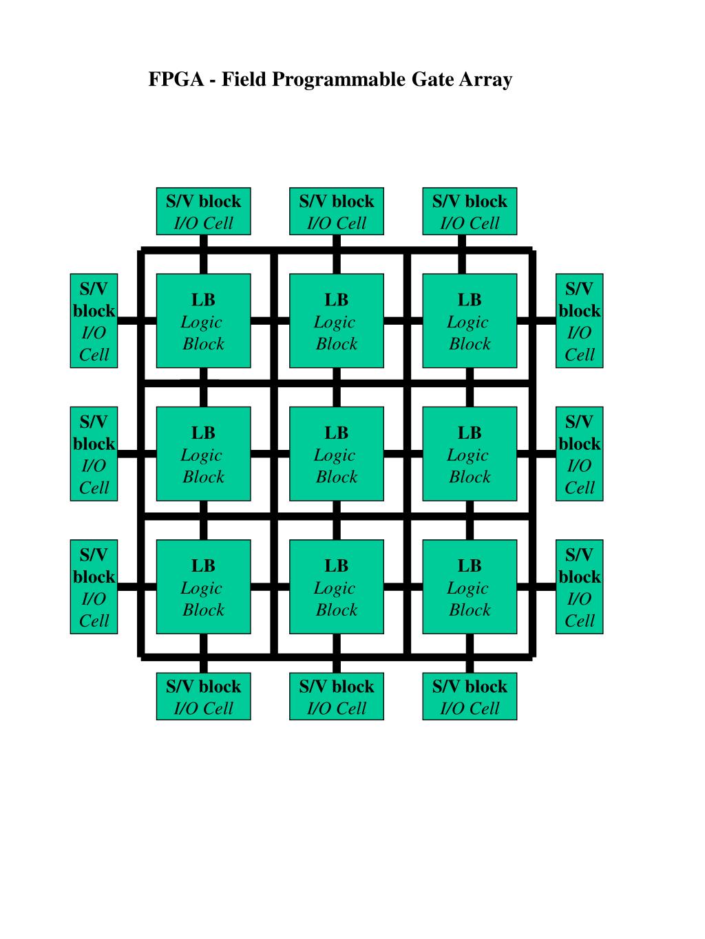
FPGA - Field Programmable Gate Array. S/V blo c k I/O Cell. S/V block I/O Cell. S/V block I/O Cell. S/V block I/O Cell. LB Logic Block. LB Logic Block. LB Logic Block. S/V block I/O Cell. S/V block I/O Cell. LB Logic Block. LB Logic Block. LB Logic Block.
FPGA - Field Programmable Gate Array - slide 1
01 / 12FPGA - Field Programmable Gate Array
1 / 17

Télécharger la présentation

FPGA - Field Programmable Gate Array
Une image / un lien ci-dessous est fourni (tel quel) pour télécharger la présentation

Politique de téléchargement : le contenu du site vous est fourni TEL QUEL pour votre information et votre usage personnel ; il ne peut être vendu, concédé sous licence ni partagé sur d’autres sites sans l’accord de son auteur.Le contenu vous est fourni TEL QUEL, pour votre information et votre usage personnel uniquement. Téléchargez la présentation en cliquant sur ce lien. Lors du téléchargement, si vous ne parvenez pas à télécharger une présentation, l’éditeur a peut-être supprimé le fichier de son serveur.Pendant le téléchargement, si vous ne parvenez pas à obtenir une présentation, le fichier a peut-être été supprimé par l’éditeur.

F I N

Plus de contenu associé

Transcription de la présentation
  1. FPGA - Field Programmable Gate Array S/V block I/O Cell S/V block I/O Cell S/V block I/O Cell S/V block I/O Cell LB Logic Block LB Logic Block LB Logic Block S/V block I/O Cell S/V block I/O Cell LB Logic Block LB Logic Block LB Logic Block S/V block I/O Cell S/V block I/O Cell LB Logic Block LB Logic Block LB Logic Block S/V block I/O Cell S/V block I/O Cell S/V block I/O Cell S/V block I/O Cell

  2. The structure of FPGA

  3. Architecture of FPGA-s Symmetrical Array Row-based LB LB LB LB LB LB LB LB LB LB LB LB LB LB LB LB LB LB LB LB LB LB LB LB Hierarchical (CPLD) Sea-of-Gates PLA PLA PLA PLA PLA PLA PLA PLA

  4. Example:realisation of the OR function based on LUT 0 1 1 X 1 1 X 2 Y 1 X 3 1 1 1 1 X 1 Y X 2 X 3

  5. Logical block based on LUT-s LUT 0 T MUX 1 S LUT 0 T MUX 1 S

  6. Example: realisation of function based on MUX-s. Y = X1 X2 + X1 X3 X1 X2 + X1 X3 X1 = 0 X1 = 1 X3 X2 X3 = 0 X2 = 1 X3 = 1 X2 = 0 0 1 1 0 MUX 0 0 1 1 X3 S MUX 0 Y X3 1 S MUX X2 1 0 X1 0 1 S X2

  7. Interconnection resources Symmetrical FPGA LB LB CB Connection arrays CB SB CB CLK Connections between the neighbours LB LB CB Long lines

  8. Row of interconnection resources in a FPGA with architecture Long lines over logical blocks LB LB LB LB LB LB For example, Actel-i Act-1, Act-2 FPGA-d

  9. Interconnection resources in Sea-of-Gates type FPGA Neighbouring connections Connections in 4x4 blocks Cell Cell Cell Cell Cell Cell Cell Cell Cell Cell Cell Cell Cell Cell Cell Cell Cell Connections in the array Connections in 16x16 blocks 4x4 cell 16x16 I/O blocks I/O b l o c k s I/O b l o c k s I/O blocks For example. XILINX XC6200 and ACTEL-i ES serial arrays

  10. Interconnection resources in CPLD type FPGA I/O blocks PLA PLA Local connection resources PLA PLA I/O blocks PLA PLA I/O blocks Local connection resource PLA PLA Global connection resource PLA Local connection resource PLA PLA PLA I/O blocks PLA PLA I/O blocks Logical block Local connection resource I/O blocks PLA PLA Macrocell

  11. I/O cells 0 MUX T 1 S S/V contact I/O pad T 0 MUX 1 S

  12. Designing of hardware based on FGPA . Description of the hardware. (Boolean functions Logical circuit, VHDL …) Logical optimization / minimisation Technology Mapping Placement Routing Programming / Configuring