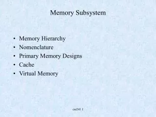
Memory Subsystem
Memory Subsystem. Memory Hierarchy Nomenclature Primary Memory Designs Cache Virtual Memory. Memory Hierarchy. Memory is organized hierarchically by size and speed usually: faster costlier, smaller slower cheaper, larger Style Speed Size registers CPU speed few 10’s

Memory Subsystem
E N D
Presentation Transcript
Memory Subsystem • Memory Hierarchy • Nomenclature • Primary Memory Designs • Cache • Virtual Memory cse241 1
Memory Hierarchy Memory is organized hierarchically by size and speed usually: faster costlier, smaller slower cheaper, larger Style Speed Size registers CPU speed few 10’s L1 (primary) cache near CPU speed few KBs (e.g., 16KB -- 128KB) L2 (secondary) cache slower than L1 KBs (256KB) Main Memory 60ns MBs (128MB -- ) On-line secondary (disk) 100MB/s GBs Off-line (tape, CD ROM etc.) -- GBs -- TBs The blue area constitutes what is usually called the “memory subsystem”. cse241 2
Semiconductor Memory Nomenclature • RAM --Random Access Memory time taken to access any arbitrary location • in memory is constant (c.f., disks) • SRAM --Static RAM A RAM chip design technology (see later) • DRAM --Dynamic RAM A RAM chip design technology (see later) • ROM --Read Only Memory ROMs are RAMs with data built-in when the • chip is created. Usually stores BIOS info. • Older uses included storage of bootstrap info • PROM --Programmable ROM A ROM which can be bench programmed • EPROM --Erasable PROM A PROM which can be bench programmed, erased • by exposure to UV radiation • EEPROM – Electrically erasable PROM • IGCMOSFET-EEPROM cse241 3
Other Nomenclature There are a lot of these acronyms. Here are a few of the more common ones. SIMM Single In-Line Memory Module A packaging technology (single 32-bit data path) DIMM Dual In-Line Memory Module A packaging technology (dual 32-bit data paths) FPM RAM Fast Page-Mode RAM An older technology capable of about 60ns cycle time EDO RAM Extended-data-out RAM More modern FPM RAM, exploiting address coherency (see cachelater) capable of about 20ns access speed SDRAM Synchronous DRAM Synchronous Dynamic RAM; allows access speeds as low as about 10ns cse241 4
Static vs Dynamic RAM Static and dynamic RAMs are two different technologies implementing the basic RAM functionality. A static RAM (SRAM) is a device which can retain its state (the contents of the RAM) as long as power is applied to the device Of course, SRAMs lose their contents when power is removed. SRAMs are usually characterized by (relatively) low density (bits per chip) but fast access (but see technology changes to DRAMs) Low power: current flows only when memory cell value changes A dynamic RAM (DRAM) is a device which must employ special designs to retain their state, even if the power to them is kept on. One way to view DRAMs is that the cells of the DRAM are capacitors which eventually lose their charge unless they are replenished. A DRAM employs special refresh circuitry which replenishes the contents of the DRAM during its operation. cse241 5
A Typical SRAM The diagram below shows a typical SRAM (a T14M1024A 128K x 8 SRAM). It has a read and a write cycle of 10, 12 or 15ns (depending on the chip you buy). 17 address lines A0 -- A16 8 data I/O lines /CE1 CE2 /WE /OE cse241 6
Functionality The T14M1024A functions as follows:- /CE1 CE2 /OE /WE Mode IO0--IO7 H X X X not selected hi-Z X L X X not selected hi-Z L H H H output disable hi-Z L H L H Read Data Out L H X L Write Data In Notice that some signals are active low (CE1, OE and WE). Note that /CE1 and CE2 select the chip Compare /OE to /CE1 and CE2. Can you see the difference? cse241 7
a simple 128K x 8 memory Address Bus (17 bits) Data Bus (8 bits) Control Bus (8 bits) 17 address lines A0 -- A16 8 Data Lines Write Read /OE /WE cse241 8
6 7 G1 Y7 4 9 G2A Y6 5 10 G2B Y5 11 138 Y4 3 12 C Y3 2 13 B Y2 1 14 A Y1 15 Y0 Decoders Remember that a decoder has n input lines and 2n output lines labeled 0 to 2n - 1; the decoder will set an active-high 1 (or active low 0) onto the output line labeled k if the binary value k appears on the n input lines. Below is a 3-to-8 decoder with active low outputs:- InputsOutputs G1 G2 A B C Y0 Y1 Y2 Y3 Y4 Y5 Y6 Y7 - H - - - H H H H H H H H L - - - - H H H H H H H H H L L L L L H H H H H H H H L L L H H L H H H H H H H L L H L H H L H H H H H H L L H H H H H L H H H H H L H L L H H H H L H H H H L H L H H H H H H L H H H L H H L H H H H H H L H H L H H H H H H H H H H L G2 = G2A + G2B cse241 9
a 256K x 8 memory Suppose we build a 256K x 8 memory; we will need two 128K x 8 chips. One will hold the lower 128K of memory (addresses 0 -- 128K -1) the other will hold the upper 128K of memory (addresses 128K -- 256K -1) We will need 18 address bits (218 = 256K) The top address bit (bit A17) will decide which block of memory (lower or upper 128K) to select Remember that the device is selected when CE1 = L and CE2 = H. cse241 10
A simple 1-stage decoded 256K memory Address bus bits A0 -- A16 (17 bits == 128K) Data Lines D0-D7 Read Write Note:- 1: The two chips share the lower 17 bits of address (which provide the addressing of the chip’s 128K of memory) 2: Address bit 17 selects the top or the bottom chip (by driving CE1/ and CE2 on both chips) 3: Notice the additional inverter 4: WC and RC are used as before 5: Note that the values of CE1/CE2 select which chip will be active; UNLESS THE CHIP IS SELECTED IT WILL NOT RESPOND TO A READ OR A WRITE COMMAND, AND ITS OUTPUTS WILL BE IN THE HI-Z CONDITION Address bus bit A17 OE WE CE1 CE2 OE WE CE1 CE2 cse241 11
Building a 1MB memory Suppose we build a 1MB memory from the 128KB chips; we would need 8 such chips (8X128K = 1M), and each chip would hold 128K of the 1M memory: This will be chip 0 This will be chip 1 This will be chip 7 The address space is partitioned into 128K blocks; block 0 has addresses 0 -- 128K -1 block 1 has addresses 128K -- 256K-1 block 2 has addresses 256K -- 384K -1 : : : : block 7 has addresses 896K -- 1024K -1 How many address bits are there? How many chip-select bits are there? cse241 12
Address decoder design The idea here is the same as it was in the previous design; we will use the address to select a 128K chip as the active (read/write) chip. 1MB requires 20 bits of address, and this address is divided as follows:- Bits 19 -- 17 (3 address bits) Bits 16 -- 0 (17 address bits) These 17 bits select the address in each 128KB block (== each chip) These 3 address bits select on of the 8 128KB blocks (chips) cse241 13
A simpler RAM chip Suppose we assume a simpler 128KB RAM chip i.e., the following:- 8 data lines 17 address lines /CS /WE /CS /WE Function Data Lines H X not selected Hi-Z L H Read data at location on address lines L L Write write data on data lines to address on address lines cse241 14
1MB memory 20 Address Lines 17 Address Lines A16 -- A0 Write Notice that the read command (RC) appears to have no effect. A slightly better design might disable the chips completely unless either RC or WC is asserted. 3 Address Lines A19--A17 3-to-8 decoder /WE Data Lines cse241 15
1MB memory 20 Address Lines Write 17 Address Lines A16 -- A0 In this design, note that we assume that the decoder can be enabled i.e., we will assume that the outputs of the decoder are always H unless the enable signal E is a 1. This way, no chip can be selected unless either Write or Read is active. Read 3 Address Lines A19--A17 3-to-8 decoder EN Data Lines cse241 16 WE
Effect of Address Partition Bits 19 -- 17 (3 address bits) Bits 16 -- 0 (17 address bits) Notice that the effect of partitioning the address bits as above is to keep contiguous memory addresses (128KB blocks of them) in the same block But consider this partition:- 17 address bits A19--A13 3 address bits A2..A0 Suppose we use the lower 3 bits to select the block, not the upper 3 bits. How does this effect the way addresses are partitioned? (Or, how would you describe where consecutive memory addresses are located?) cse241 17
Interleaving 17 address bits A19--A13 3 addr bits A2..A0 0 1 2 3 4 5 6 7 value in the lower 3 bits: 000 001 010 011 100 101 110 111 selects the block of 128K in which the address resides. Thus, block 0 has address 0 8 16… block 1 has address 1 9 17… block 2 has address 2 10 18… block 3 has address 3 11 19… block 4 has address 4 12 20… block 5 has address 5 13 21… block 6 has address 6 14 22… block 7 has address 7 15 23… cse241 18
Interleaved memory It is important to note the difference between interleaved and non-interleaved memory:- Interleaved: consecutive addresses are in consecutive memory blocks a block failure will leave gaps (missing addresses) distributed throughout memory but if we could organize the read/write mechanism to read or write to blocks independently, then we could speed up memory accesses by allowing overlapped fetches Non-Interleaved: consecutive addresses are in the same memory block a block failure just removes a contiguous block of memory (this can be easily compensated for) but we could not exploit the parallel fetching process cse241 19
The Principle of Locality of Reference A very important principle, underpinning --EDO RAM design --interleaved memory with overlapped access --cache Principle: If a data word (instruction) has been fetched from address K, then the likelihood that the next data word (instruction) is in the next sequential memory address is high Observation: Obviously, this is program/data dependent. But it holds up well in practice. cse241 20
Overlapped Fetches in Interleaved Memory Suppose the diagram above represents 8 blocks of interleaved memory, so that addresses are distributed as: K in block 0, K+1 in block 1, K+2 in block 2,...., K+7 in block 7 etc. Remember that a memory read cycle is composed of 3 basic parts 1) place address on address bus 2) memory read cycle 3) read data from data bus Non-overlapped memory accesses look like this:- However, we could overlap the memory accesses like this is we had an interleaved memory:- cse241 21
Overlapped Fetches in Interleaved Memory To get these fetches to overlap, we would need a) to place an address on the address bus and have the addressed memory module “latch” (save) it b) remove that address during that memory module’s read cycle c) during that time slot, place the address of the next location (in a different memory module) on the address bus --and so on We could then read data from the data bus by keeping track of when we expect to see a data word appear on the data bus cse241 22
Generic Memory System (simplified) System Bus (Address/Data/Control) Data Rd, Wt M e m o r y A r r a y XACK Block Select Decoder XACK generate logic Chip Selects WE/OE Command Decode Logic cse241 23