Introduction to CMOS Process Technology: A Comprehensive Overview
530 likes | 827 Vues
This comprehensive guide provides an overview of CMOS process technology, covering topics such as Si semiconductor technology, basic CMOS technology, layout design rules, latch-up effect, and more. Discover the intricate process flow, from oxidation to diffusion, and gain insights into wafer processing techniques. Learn about masking materials, self-alignment processes, and major IC manufacturing flows. With detailed illustrations and explanations, this resource offers valuable insights for students and professionals in the field of electronic engineering.

Introduction to CMOS Process Technology: A Comprehensive Overview
E N D
Presentation Transcript
Introduction to IC Design Tsung-Chu Huang (黃宗柱) Department of Electronic Eng. Chong Chou Institute of Tech. Email: tch@dragon.ccut.edu.tw 2003/10/13
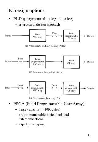
CMOS Process Tech • Si Semiconductor Technology • Basic CMOS Technology • CMOS Process • Layout Design Rules • Latchup Effect • Extractor & DRC • An n-Well CMOS Process Flow • CIC Tape-In Flow & Tutorial
CMOS Process Tech • Oxidation (氧化) • Epitaxy (磊晶) • Deposition (沉積) • Implantation (植入) • Diffusion (擴散)
Wafer Processing mm/min 1425°C Czochralski’s Method
Wafer Treatments • Grinding • Slicing • Lapping • Etching • Polishing • Cleaning • Inspection
Wafer Size 16” 12” 8” 6” 3” 1970 1980 1990 2000 2010
Oxidation Wet Dry O2 O2 1200°C H2O 900°C
Chemical Vapor Deposition Impurity Vapor (e.g., Ga, In) P Substrate
Epitaxy Si Vapor Single Crystal
Diffusion Impurity
Iron Implantation Impurity Iron • Previously used to adjust the threshold voltage; • Currently usually used to be active region.
Common Material Used As Masks • Photoresist • Polysilicon • Silicon Dioxide • Silicon Nitride
Masking using PR UV Solvant 1 Photo Masking Coating with a PR Sloved after the process using the mask Self-Align: if the rest mask is also a useful layer.
Basic CMOS Technology • N-Well Process • P-Well Process • Twin-Well (Twin-Tub) Process • Silicon on Insulator
Major IC Manufacture Flow • 電路設計 • 〈IC design〉 • 晶圓加工 • 〈wafer fabrication, FAB〉 • 封裝 • 〈packaging〉 • 測試 • 〈test〉
A Detailed MOS Process Courtesy of Chuang, “VLSI Technology,” ISBN:957-584-327-4 .
電晶體簡化佈局流程 決定“閘”(Gate)的長與寬 寬 W 長 L 薄氧化層 Thinox 決定工作區域(Active Region) 上視圖 剖面圖
電晶體簡化佈局流程 遮照 Mask 厚氧化層 Thick Oxide 剖面圖
電晶體簡化佈局流程 遮罩 Mask 剖面圖
電晶體簡化佈局流程 擴散(Diffusion) 或 離子植入(Implant)區 上視圖 剖面圖
電晶體簡化佈局流程 上視圖 決定電晶體是 P 或 N 型
以一個Not gate加以說明 上視圖 P型電晶體 N型電晶體 電子移動率Mobility, m ~ 1 : 2.6 通常,為了讓Noise margin平衡,或使NOT閘的臨界電壓折中: P型電晶體的W/L常為N型的2到3倍!
N-Well製程 金屬, Al 或 Cu, Metal P+ P+ N+ N+ 上視圖 N+ Imp, 高濃度N型植入 P+ Imp, 高濃度P型植入 剖面圖 N-Bulk P-Substrate
N-Well製程 上視圖 剖面圖 N Well
Latch-up Effect in n-Well Process Vss IN 上視圖 OUT Vdd 剖面圖 Latch up ! 正回授鎖死而燒毀!
Preventing Latch-up • Using Twin-Well (雙井製程) • Evolved in DRC • 每個N-Well要有N-型Contact接Vdd • 近Source-gate(源極) • 一般5~10個電晶體最少加一個Well Contact • 有的Rule甚至要求一個電晶體加一個Well contact
Contact Basic 4 Layers:
Via Metal 2 Metal 1 The widths of a via or contact are much sensitive to the process so that they are usually optimized to a constant, say 0.4um in 0.35um technology.
Local Interconnections Diffusion as interconnection: • Diffusion: < 1 Transistor • N-Well: < 1~5 Transistors • Polysilicon: 1~5 Transistors
SAlicide Silicide: a refractory metal, e.g., Si+Ta, Rs~1 Polysilicon Process Polysilicon: a multi-crystal semiconductor, Rs~10 Silicide Process Polycide Process Self-Aligned Polycide Process
Thin Film Process SOI Process Thin Film Transistor (TFT) Hi-density memory, Flat-Panel Display
Silicon on Insulator (SOI) Transistor(s) Without Inter-leakage Transistor(s) Without Inter-leakage P bulk N bulk Sapphire (藍寶石)
Design Rule Check (DRC) • Geometrical • X-Y Plane: Single-Layer Layout • Z Plane: Interactions btw Layers • ERC • Electrical Rule Check • Custom Rules
Scaling l 1 C=K C=lK • Linear Scaling
Scaling l 1 A=K A=l2K • First Order Scaling
Basic Categories of Rules • Micron (m) Rules • Listing all min. feature sizes in m’s • Re-listing is required after scaling. • Lambda (l) Rules • The min. active width = 1 l (mm). • Linear Scaling by l (l/m Rule). • First Order Scaling. • Must be modified in another range.
Basic Parameters in DRC Spacing Extend Width
Some Related Terminology Circuit Extractor Logic Extractor
Basic CIC Tape-In Flow Customer Transaction Extract Designer Layout Engineer Frontend HDL, Sch Netlist… HDL, Sch Netlist… LVS Simulation Backend Foundry DRC Tape-In Tape-Out
Reverse Engineering (RE) • Category • Mechanism • Software: database, programming • VLSI: layout • Purpose: • Failure inspection • Amoral hack, referring • Illegal stealing (duplication)
VLSI RE Flow • Unpacking • Chemical Metal Polishing (CMP) • Photographing • Inspection • Schematic • Simulation & Verification
Reversing Rule Check Layout DRC LVS Layout DRC Schematic Inspection Simulation Forward Engineering: Schematic Reverse Engineering: Photo